TPS929160-Q1
ZHCSNG0 – APRIL 2023
www.ti.com.cn
Return to the Summary Table.
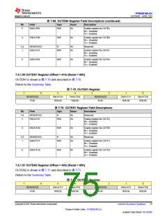
图 7-74. IOUTA0 Register
7
6
5
4
3
2
1
1
1
0
0
0
RESERVED
R-0h
IOUTA0
R/W-X
表 7-76. IOUTA0 Register Field Descriptions
Bit
Field
Type
Reset
Description
7-6
5-0
RESERVED
IOUTA0
R
0h
Reserved
R/W
X
Output current setting for OUTA0
Load EEPROM register data when reset
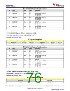
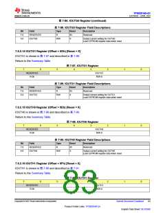
7.6.2.2 IOUTA1 Register (Offset = 51h) [Reset = X]
IOUTA1 is shown in 图 7-75 and described in 表 7-77.
Return to the Summary Table.
图 7-75. IOUTA1 Register
7
6
5
4
3
2
RESERVED
R-0h
IOUTA1
R/W-X
表 7-77. IOUTA1 Register Field Descriptions
Bit
Field
Type
Reset
Description
7-6
5-0
RESERVED
IOUTA1
R
0h
Reserved
R/W
X
Output current setting for OUTA1
Load EEPROM register data when reset
7.6.2.3 IOUTB0 Register (Offset = 52h) [Reset = X]
IOUTB0 is shown in 图 7-76 and described in 表 7-78.
Return to the Summary Table.
图 7-76. IOUTB0 Register
7
6
5
4
3
2
RESERVED
R-0h
IOUTB0
R/W-X
表 7-78. IOUTB0 Register Field Descriptions
Bit
Field
Type
Reset
Description
7-6
5-0
RESERVED
IOUTB0
R
0h
Reserved
R/W
X
Output current setting for OUTB0
Load EEPROM register data when reset
7.6.2.4 IOUTB1 Register (Offset = 53h) [Reset = X]
IOUTB1 is shown in 图 7-77 and described in 表 7-79.
Return to the Summary Table.
Copyright © 2023 Texas Instruments Incorporated
Submit Document Feedback
79
Product Folder Links: TPS929160-Q1
English Data Sheet: SLVSG60

 TI [ TEXAS INSTRUMENTS ]