TPS65910, TPS65910A, TPS65910A3, TPS659101, TPS659102, TPS659103
TPS659104, TPS659105, TPS659106, TPS659107, TPS659108, TPS659109
www.ti.com
SWCS046N –MARCH 2010–REVISED APRIL 2012
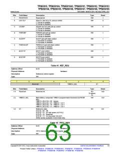
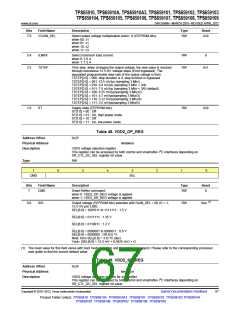
Bits
Field Name
Description
Type
Reset
7:6
VGAIN_SEL
Select output voltage multiplication factor: G (EEPROM bits):
RW
0x0
when 00: x1
when 01: x1
when 10: x2
when 11: x3
5:4
3:2
ILMAX
TSTEP
Select maximum load current:
when 0: 1.0 A
when 1: 1.5 A
RW
RW
0
Time step: when changing the output voltage, the new value is reached
through successive 12.5 mV voltage steps (if not bypassed). The
equivalent programmable slew rate of the output voltage is then:
TSTEP[2:0] = 000: step duration is 0, step function is bypassed
TSTEP[2:0] = 001: 12.5 mV/µs (sampling 3 Mhz)
0x1
TSTEP[2:0] = 010: 9.4 mV/µs (sampling 3 Mhz × 3/4)
TSTEP[2:0] = 011: 7.5 mV/µs (sampling 3 Mhz × 3/5) (default)
TSTEP[2:0] = 100: 6.25 mV/µs(sampling 3 Mhz/2)
TSTEP[2:0] = 101: 4.7 mV/µs(sampling 3 Mhz/3)
TSTEP[2:0] = 110: 3.12 mV/µs(sampling 3 Mhz/4)
TSTEP[2:0] = 111: 2.5 mV/µs(sampling 3 Mhz/5)
1:0
ST
Supply state (EEPROM bits):
ST[1:0] = 00 : Off
RW
0x0
ST[1:0] = 01 : On, high power mode
ST[1:0] = 10 : Off
ST[1:0] = 11 : On, low power mode
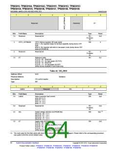
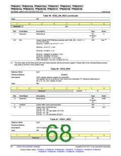
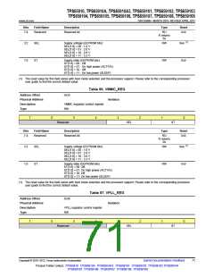
Table 48. VDD2_OP_REG
Address Offset
Physical Address
Description
0x25
Instance
VDD2 voltage selection register.
This register can be accessed by both control and smartreflex I2C interfaces depending on
SR_CTL_I2C_SEL register bit value.
Type
RW
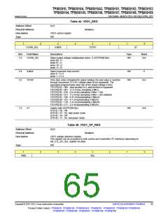
7
6
5
4
3
2
1
0
CMD
SEL
Bits
Field Name
Description
Type
Reset
7
CMD
Smart-Reflex command:
RW
0
when 0: VDD2_OP_REG voltage is applied
when 1: VDD2_SR_REG voltage is applied
(1)
6:0
SEL
Output voltage (EEPROM bits) selection with GAIN_SEL = 00 (G = 1,
RW
See
12.5 mV per LSB):
SEL[6:0] = 1001011 to 1111111 : 1.5 V
...
SEL[6:0] = 0111111 : 1.35 V
...
SEL[6:0] = 0110011 : 1.2 V
...
SEL[6:0] = 0000001 to 0000011 : 0.6 V
SEL[6:0] = 0000000 : Off (0.0 V)
Note: from SEL[6:0] = 3 to 75 (dec)
Vout= (SEL[6:0] × 12.5 mV + 0.5625 mV) × G
(1) The reset value for this field varies with boot mode selection and the processor support. Please refer to the corresponding processor
user guide to find the correct default value.
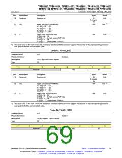
Table 49. VDD2_SR_REG
Address Offset
Physical Address
Description
0x26
Instance
VDD2 voltage selection register for smartreflex.
This register can be accessed by both control and smartreflex I2C interfaces depending on
SR_CTL_I2C_SEL register bit value.
Copyright © 2010–2012, Texas Instruments Incorporated
Submit Documentation Feedback
67
Product Folder Link(s): TPS65910 TPS65910A TPS65910A3 TPS659101 TPS659102 TPS659103 TPS659104
TPS659105 TPS659106 TPS659107 TPS659108 TPS659109

 TI [ TEXAS INSTRUMENTS ]