TPS65910, TPS65910A, TPS65910A3, TPS659101, TPS659102, TPS659103
TPS659104, TPS659105, TPS659106, TPS659107, TPS659108, TPS659109
www.ti.com
SWCS046N –MARCH 2010–REVISED APRIL 2012
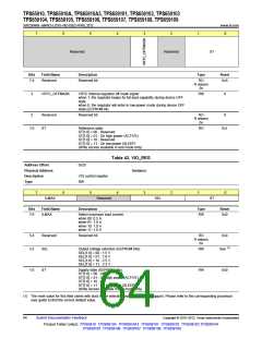
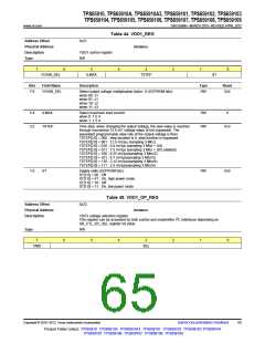
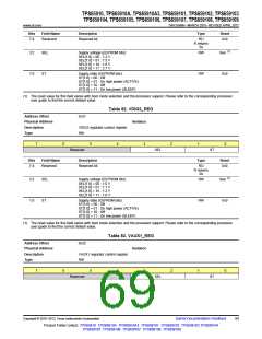
Table 44. VDD1_REG
Address Offset
Physical Address
Description
Type
0x21
Instance
VDD1 control register
RW
7
6
5
4
3
2
1
0
VGAIN_SEL
ILMAX
TSTEP
ST
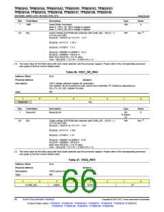
Bits
Field Name
Description
Type
Reset
7:6
VGAIN_SEL
Select output voltage multiplication factor: G (EEPROM bits):
RW
0x0
when 00: x1
when 01: x1
when 10: x2
when 11: x3
5:4
3:2
ILMAX
TSTEP
Select maximum load current:
when 0: 1.0 A
when 1: 1.5 A
RW
RW
0
Time step: when changing the output voltage, the new value is reached
through successive 12.5 mV voltage steps (if not bypassed). The
equivalent programmable slew rate of the output voltage is then:
TSTEP[2:0] = 000 : step duration is 0, step function is bypassed
TSTEP[2:0] = 001 : 12.5 mV/µs (sampling 3 Mhz)
0x3
TSTEP[2:0] = 010 : 9.4 mV/µs (sampling 3 Mhz × 3/4)
TSTEP[2:0] = 011 : 7.5 mV/µs (sampling 3 Mhz × 3/5) (default)
TSTEP[2:0] = 100 : 6.25 mV/µs(sampling 3 Mhz/2)
TSTEP[2:0] = 101 : 4.7 mV/µs(sampling 3 Mhz/3)
TSTEP[2:0] = 110 : 3.12 mV/µs(sampling 3 Mhz/4)
TSTEP[2:0] = 111 : 2.5 mV/µs(sampling 3 Mhz/5)
1:0
ST
Supply state (EEPROM bits):
ST[1:0] = 00 : Off
RW
0x0
ST[1:0] = 01 : On, high power mode
ST[1:0] = 10 : Off
ST[1:0] = 11 : On, low power mode
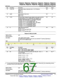
Table 45. VDD1_OP_REG
Address Offset
Physical Address
Description
0x22
Instance
VDD1 voltage selection register.
This register can be accessed by both control and smartreflex I2C interfaces depending on
SR_CTL_I2C_SEL register bit value.
Type
RW
7
6
5
4
3
2
1
0
CMD
SEL
Copyright © 2010–2012, Texas Instruments Incorporated
Submit Documentation Feedback
65
Product Folder Link(s): TPS65910 TPS65910A TPS65910A3 TPS659101 TPS659102 TPS659103 TPS659104
TPS659105 TPS659106 TPS659107 TPS659108 TPS659109

 TI [ TEXAS INSTRUMENTS ]