TPS65910, TPS65910A, TPS65910A3, TPS659101, TPS659102, TPS659103
TPS659104, TPS659105, TPS659106, TPS659107, TPS659108, TPS659109
www.ti.com
SWCS046N –MARCH 2010–REVISED APRIL 2012
Bits
Field Name
Description
Type
Reset
7:4
Reserved
Reserved bit
RO
R returns
0s
0x0
(1)
3:2
1:0
SEL
ST
Supply voltage (EEPROM bits):
SEL[1:0] = 00 : 1.2 V
SEL[1:0] = 01 : 1.5 V
SEL[1:0] = 10 : 1.8 V
SEL[1:0] = 11 : 2.7 V
RW
See
Supply state (EEPROM bits):
ST[1:0] = 00 : Off
RW
0x0
ST[1:0] = 01 : On high power (ACTIVE)
ST[1:0] = 10 : Off
ST[1:0] = 11 : On low power (SLEEP)
(1) The reset value for this field varies with boot mode selection and the processor support. Please refer to the corresponding processor
user guide to find the correct default value.
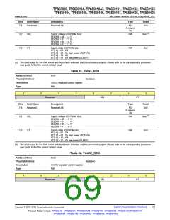
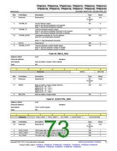
Table 52. VDIG2_REG
Address Offset
Physical Address
Description
Type
0x31
Instance
VDIG2 regulator control register
RW
7
6
5
4
3
2
1
0
Reserved
SEL
ST
Bits
Field Name
Description
Type
Reset
7:4
Reserved
Reserved bit
RO
R returns
0s
0x0
(1)
3:2
1:0
SEL
Supply voltage (EEPROM bits):
SEL[1:0] = 00 : 1.0 V
SEL[1:0] = 01 : 1.1 V
SEL[1:0] = 10 : 1.2 V
SEL[1:0] = 11 : 1.8 V
RW
See
ST
Supply state (EEPROM bits):
ST[1:0] = 00 : Off
RW
0x0
ST[1:0] = 01 : On high power (ACTIVE)
ST[1:0] = 10 : Off
ST[1:0] = 11 : On low power (SLEEP)
(1) The reset value for this field varies with boot mode selection and the processor support. Please refer to the corresponding processor
user guide to find the correct default value.
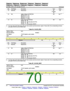
Table 53. VAUX1_REG
Address Offset
Physical Address
Description
Type
0x32
Instance
VAUX1 regulator control register
RW
7
6
5
4
3
2
1
0
Reserved
SEL
ST
Copyright © 2010–2012, Texas Instruments Incorporated
Submit Documentation Feedback
69
Product Folder Link(s): TPS65910 TPS65910A TPS65910A3 TPS659101 TPS659102 TPS659103 TPS659104
TPS659105 TPS659106 TPS659107 TPS659108 TPS659109

 TI [ TEXAS INSTRUMENTS ]