TPS65163
SLVSA28 –OCTOBER 2009
www.ti.com
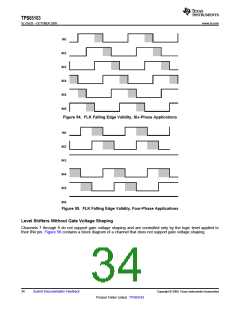
IN1
IN2
IN3
IN4
IN5
IN6
Figure 54. FLK Falling Edge Validity, Six-Phase Applications
IN1
IN2
IN3
IN4
IN5
IN6
Figure 55. FLK Falling Edge Validity, Four-Phase Applications
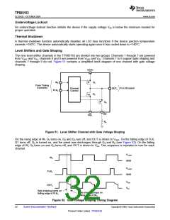
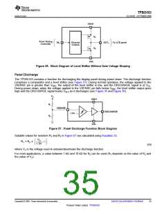
Level Shifters Without Gate Voltage Shaping
Channels 7 through 9 do not support gate voltage shaping and are controlled only by the logic level applied to
their INx pin. Figure 56 contains a block diagram of a channel that does not support gate voltage shaping.
34
Submit Documentation Feedback
Copyright © 2009, Texas Instruments Incorporated
Product Folder Link(s) :TPS65163

 TI [ TEXAS INSTRUMENTS ]