TPS65163
www.ti.com
SLVSA28 –OCTOBER 2009
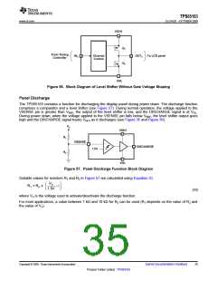
VGH1
Q1
From Timing
Controller
INX
Channel
Control
OUTX
To LCD panel
Q2
VGL
Figure 56. Block Diagram of Level Shifter Without Gate Voltage Shaping
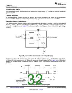
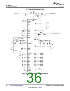
Panel Discharge
The TPS65163 contains a function for discharging the display panel during power down. The discharge function
comprises a comparator and a level shifter (see Figure 57). During normal operation, the voltage applied to the
VSENSE pin is greater than VREF, the output of the level shifter is low, and the DISCHARGE signal is at VGL
.
During power down, when the voltage applied to the VSENSE pin falls below VREF, the level shifter output goes
high and the DISCHARGE signal tracks VGH1 as it discharges (see Figure 35 and Figure 36).
VX
VGH1
R1
VSENSE
-
DISCHARGE
1.5V
+
R2
VGL
Figure 57. Panel Discharge Function Block Diagram
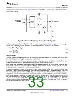
Suitable values for resistors R1 and R2 in Figure 57 are calculated using Equation 33.
VX
æ
ö
R1 = R2 x
-1
ç
÷
1.5V
è
ø
(33)
where VX is the voltage used to activate/deactivate the discharge function.
For most applications, a value between 1 kΩ and 10 kΩ for R2 can be used (R1 depends on the value of R2 and
the value of VX).
Copyright © 2009, Texas Instruments Incorporated
Submit Documentation Feedback
35
Product Folder Link(s) :TPS65163

 TI [ TEXAS INSTRUMENTS ]