TPS65163
www.ti.com
SLVSA28 –OCTOBER 2009
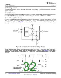
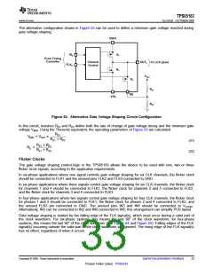
The alternative configuration shown in Figure 53 can be used to define a minimum gate voltage reached during
gate voltage shaping.
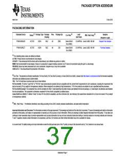
VGH1
INX
Q1
Q2
From Timing
Controller
Channel
Control
OUTX
To LCD panel
FLKX
VGH1
Q3
RE1
RE
VGL
RE2
Figure 53. Alternative Gate Voltage Shaping Circuit Configuration
In this circuit, resistors RE1 and RE2 define both the rate of change of gate voltage decay and the minimum gate
voltage VMIN. Using the Thevenin equivalent, the operating parameters of Figure 53 are calculated.
RE2
VMIN = VGH1
x
RE1 + RE2
(31)
(32)
RE1 x RE2
RE1 + RE2
RE
=
Flicker Clocks
The gate voltage shaping control logic in the TPS65163 allows the device to be used with one, two or three
flicker clock signals, according to the application requirements.
In six-phase applications where one signal controls gate voltage shaping for six CLK channels, the flicker clock
should be connected to FLK1 and the unused pins FLK2 and FLK3 connected to GND.
In six-phase applications where three signals control gate voltage shaping for six CLK channels, the flicker clock
for channels 1 and 4 should be connected to FLK1, the flicker clock for channels 2 and 5 connected to FLK2,
and the flicker clock for channels 3 and 6 connected to FLK3.
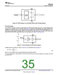
In four-phase applications where two signals control gate voltage shaping for four CLK channels, the flicker clock
for phases 1 and 3 should be connected to FLK1, the flicker clock for phases 2 and 4 connected to FLK2, and
the unused FLK3 pin connected to GND. The unused pins IN3 and IN6 should be connected to VLOGIC
.
Alternatively, IN3 can be connected to IN2 and IN6 connected to IN5; this arrangement can simplify PCB layout.
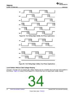
Gate voltage shaping is started by the falling edge of the FLK signal(s), which must occur during a valid part of
the clock waveform. For six-phase systems, this means the last 60° of the clock waveform; for four-phase
systems, this means the last 90° of the clock waveform (see Figure 54 and Figure 55). Falling edges of the FLK
signal(s) occurring outside the valid part of the clock waveform are ignored. The rising edge of the FLK signal(s)
has no effect, regardless of when it occurs.
Copyright © 2009, Texas Instruments Incorporated
Submit Documentation Feedback
33
Product Folder Link(s) :TPS65163

 TI [ TEXAS INSTRUMENTS ]