TPS65163
SLVSA28 –OCTOBER 2009
www.ti.com
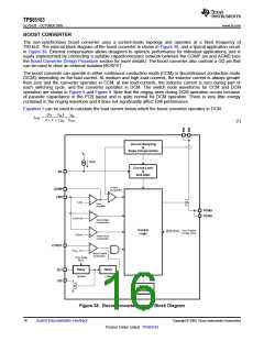
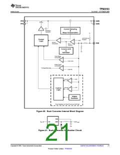
BUCK CONVERTER
The buck converter is a non-synchronous type that runs at a fixed frequency of 750 kHz. The converter features
integrated soft-start (0.66 ms), bootstrap, and compensation circuits to minimize external component count. The
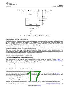
buck converter internal block diagram is shown in Figure 40, and a typical application circuit in Figure 41.
The output voltage of the buck converter is internally programmed to 3.3 V and is enabled as soon as VIN
exceeds the UVLO threshold. For best performance, the buck converter FB pin should be connected directly to
the positive terminal of the output capacitor(s).
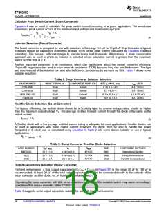
The buck converter can operate in either continuous conduction mode (CCM) or discontinuous conduction mode
(DCM), depending on the load current. At medium and high load currents, the inductor current is always greater
than zero and the converter operates in CCM; at low load currents, the inductor current is zero during part of
each switching cycle, and the converter operates in DCM. The switch node waveforms for CCM and DCM
operation are shown in Figure 11 and Figure 12. Note that the ringing seen during DCM operation occurs
because of parasitic capacitance in the PCB layout and is quite normal for DCM operation. However, there is
little energy contained in the ringing waveform, and it does not significantly affect EMI performance. Equation 10
can be used to calculate the load current below which the buck converter operates in DCM.
V
- VLOGIC
(
)
VLOGIC
IN
IDCM
=
´
2 ´ L ´ ¦SW
V
IN
(10)
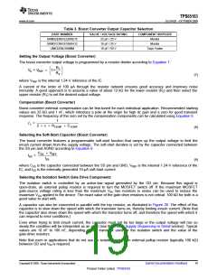
The buck converter uses a skip mode to regulate VLOGIC at low load currents. This mode allows the converter to
maintain its output at the required voltage while still meeting the requirement of a minimum on-time. The buck
converter enters skip mode when its feedback voltage exceeds the skip-mode threshold (25% above the normal
VFBB regulation voltage). During skip mode, the buck converter switches for a few cycles, then stops switching for
a few cycles, and then starts switching again, and so on, for as long as VFBB remains above the skip-mode
threshold. Output voltage ripple can be higher during skip mode (see Figure 13).
20
Submit Documentation Feedback
Copyright © 2009, Texas Instruments Incorporated
Product Folder Link(s) :TPS65163

 TI [ TEXAS INSTRUMENTS ]
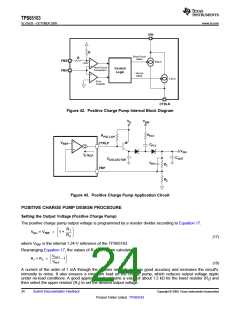