TPS65163
www.ti.com
SLVSA28 –OCTOBER 2009
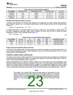
Table 3. Boost Converter Output Capacitor Selection
PART NUMBER
VALUE / VOLTAGE RATING
22 µF / 25 V
COMPONENT SUPPLIER
GRM32ER61E226KE15
GRM31CR61E106KA12
UMK325BJ106MM
Murata
Murata
10 µF / 25 V
10 µF / 50 V
Taiyo Yuden
Setting the Output Voltage (Boost Converter)
The boost converter output voltage is programmed by a resistor divider according to Equation 7.
æ
ç
è
R1 ö
VS = VREF
´
1+
÷
R2 ø
(7)
where VREF is the internal 1.24-V reference of the IC.
A current of the order of 100 µA through the resistor network ensures good accuracy and improves noise
immunity. A good approach is to assume a value of about 12 kΩ for the lower resistor (R2) and then select the
upper resistor (R1) to set the desired output voltage.
Compensation (Boost Converter)
Boost converter external compensation can be fine-tuned for each individual application. Recommended starting
values are 33 kΩ and 1 nF, which introduce a pole at the origin for high dc gain and a zero for good transient
response. The frequency of the zero set by the compensation components can be calculated using Equation 8.
1
¦
=
z
2 ´ p ´ RCOMP ´ CCOMP
(8)
Selecting the Soft-Start Capacitor (Boost Converter)
The boost converter features a programmable soft-start function that ramps up the output voltage to limit the
inrush current drawn from the supply voltage. The soft-start duration is set by the capacitor connected between
the SS pin and AGND according to Equation 9.
CSS ´ VREF
tSS
=
ISS
(9)
where CSS is the capacitor connected between the SS pin and GND, VREF is the internal 1.24-V reference of the
IC, and ISS is the internally generated 10-µA soft-start current.
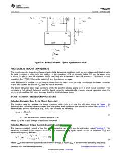
Selecting the Isolation Switch Gate Drive Components
The isolation switch is controlled by an active-low signal generated by the GD pin. Because this signal is
open-drain, an external pullup resistor is required to turn the MOSFET switch off. If the maximum MOSFET
gate-source voltage rating is less than the maximum VIN, two resistors in series can be used to reduce the
maximum VGS applied to the device. The exact value of the gate drive resistors is not critical: 100 kΩ for both is a
good value to start with.
A capacitor can also be connected in parallel with the top resistor, as illustrated in Figure 39. The effect of this
capacitor is to slow down the speed with which the transistor turns on, thereby limiting inrush current. (Note that
the capacitor also slows down the speed with which the transistor turns off, and therefore the speed with which it
can respond to error conditions.)
Even when trying to limit inrush current, the capacitor must not be too large or the output voltage will rise so
slowly the condition will be interpreted as an error (see the Power Supply Sequencing in Detail section). Typical
values are 10 nF to 100 nF, depending on the transistor used for the isolation switch and the value of the
gate-drive resistors.
Note that even in applications that do not use an isolation switch, an external pullup resistor (typically 100 kΩ)
between GD and VIN is required.
Copyright © 2009, Texas Instruments Incorporated
Submit Documentation Feedback
19
Product Folder Link(s) :TPS65163

 TI [ TEXAS INSTRUMENTS ]