TPS65163
SLVSA28 –OCTOBER 2009
www.ti.com
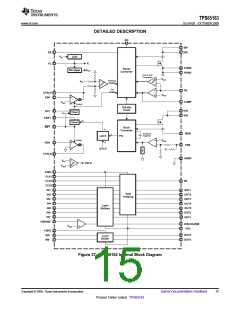
BOOST CONVERTER
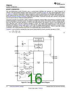
The non-synchronous boost converter uses a current-mode topology and operates at a fixed frequency of
750 kHz. The internal block diagram of the boost converter is shown in Figure 38, and a typical application circuit
in Figure 39. External compensation allows designers to optimize performance for individual applications, and is
easily implemented by connecting a suitable capacitor/resistor network between the COMP pin and AGND (see
the Boost Converter Design Procedure section for more details). The boost converter also controls a GD pin that
can be used to drive an external isolation MOSFET.
The boost converter can operate in either continuous conduction mode (CCM) or discontinuous conduction mode
(DCM), depending on the load current. At medium and high load currents, the inductor current is always greater
than zero and the converter operates in CCM; at low load currents, the inductor current is zero during part of
each switching cycle, and the converter operates in DCM. The switch node waveforms for CCM and DCM
operation are shown in Figure 5 and Figure 6. Note that the ringing seen during DCM operation occurs because
of parasitic capacitance in the PCB layout and is quite normal for DCM operation. There is very little energy
contained in the ringing waveform and it does not significantly affect EMI performance.
Equation 1 can be used to calculate the load current below which the boost converter operates in DCM.
V
- V
IN
(
)
2 ´ L ´ ¦SW VO UT
V
IN
S
IDCM
=
´
(1)
Current Sampling
&
Slope Compensation
VL
10µA
Current Limit
&
Soft-Start
SS
Current
Comparator
COMP
FBP
+
-
-
1.24V
+
Error
Amplifier
PGND
PGND
+
-
1.24V+3%
Overvoltage
Comparator
-
Control
Logic
Short-Circuit From Positive
Charge Pump
200mV
+
Short-Circuit
Comparator
+
-
CTRLP
≈(V - 2V)
IN
Boost Enable
Comparator
From Reset
Block
Delay
Delay
DLY
GD
Variable
1.36ms
750kHz
Oscillator
Figure 38. Boost Converter Internal Block Diagram
16
Submit Documentation Feedback
Copyright © 2009, Texas Instruments Incorporated
Product Folder Link(s) :TPS65163

 TI [ TEXAS INSTRUMENTS ]