TPS54560
www.ti.com
SLVSBN0 –MARCH 2013
DETAILED DESCRIPTION (continued)
æ
ç
ö
IO ´Rdc + VOUT + Vd
1
÷
fSW maxskip
=
´
(
)
ç
÷
tON
VIN -IO ´RDS on + Vd
( )
è
ø
(7)
(8)
æ
ö
÷
ICL ´Rdc + VOUT sc + Vd
fDIV
( )
ç
fSW(shift)
=
´
ç
÷
tON
VIN -ICL ´RDS on + Vd
( )
è
ø
IO
Output current
ICL
Current limit
Rdc
VIN
VOUT
inductor resistance
maximum input voltage
output voltage
VOUTSC
Vd
output voltage during short
diode voltage drop
RDS(on)
tON
switch on resistance
controllable on time
ƒDIV
frequency divide equals (1, 2, 4, or 8)
Synchronization to RT/CLK Pin
The RT/CLK pin can receive a frequency synchronization signal from an external system clock. To implement
this synchronization feature connect a square wave to the RT/CLK pin through either circuit network shown in
Figure 27. The square wave applied to the RT/CLK pin must switch lower than 0.5 V and higher than 1.7 V and
have a pulsewidth greater than 15 ns. The synchronization frequency range is 160 kHz to 2300 kHz. The rising
edge of the SW will be synchronized to the falling edge of RT/CLK pin signal. The external synchronization circuit
should be designed such that the default frequency set resistor is connected from the RT/CLK pin to ground
when the synchronization signal is off. When using a low impedance signal source, the frequency set resistor is
connected in parallel with an ac coupling capacitor to a termination resistor (e.g., 50 Ω) as shown in Figure 27.
The two resistors in series provide the default frequency setting resistance when the signal source is turned off.
The sum of the resistance should set the switching frequency close to the external CLK frequency. It is
recommended to ac couple the synchronization signal through a 10 pF ceramic capacitor to RT/CLK pin.
The first time the RT/CLK is pulled above the PLL threshold the TPS54560 switches from the RT resistor free-
running frequency mode to the PLL synchronized mode. The internal 0.5 V voltage source is removed and the
RT/CLK pin becomes high impedance as the PLL starts to lock onto the external signal. The switching frequency
can be higher or lower than the frequency set with the RT/CLK resistor. The device transitions from the resistor
mode to the PLL mode and locks onto the external clock frequency within 78 microseconds. During the transition
from the PLL mode to the resistor programmed mode, the switching frequency will fall to 150 kHz and then
increase or decrease to the resistor programmed frequency when the 0.5 V bias voltage is reapplied to the
RT/CLK resistor.
The switching frequency is divided by 8, 4, 2, and 1 as the FB pin voltage ramps from 0 to 0.8 volts. The device
implements a digital frequency foldback to enable synchronizing to an external clock during normal start-up and
fault conditions. Figure 28, Figure 29 and Figure 30 show the device synchronized to an external system clock in
continuous conduction mode (CCM), discontinuous conduction (DCM), and pulse skip mode (Eco-Mode).
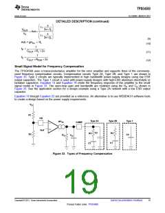
SPACER
Copyright © 2013, Texas Instruments Incorporated
Submit Documentation Feedback
15
Product Folder Links: TPS54560

 TI [ TEXAS INSTRUMENTS ]