TPS54560
SLVSBN0 –MARCH 2013
www.ti.com
DETAILED DESCRIPTION (continued)
Selecting the Switching Frequency
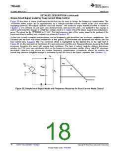
The TPS54560 implements peak current mode control in which the COMP pin voltage controls the peak current
of the high side MOSFET. A signal proportional to the high side switch current and the COMP pin voltage are
compared each cycle. When the peak switch current intersects the COMP control voltage, the high side switch is
turned off. During overcurrent conditions that pull the output voltage low, the error amplifier increases switch
current by driving the COMP pin high. The error amplifier output is clamped internally at a level which sets the
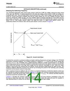
peak switch current limit. The TPS54560 provides an accurate current limit threshold with a typical current limit
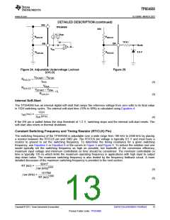
delay of 60 ns. With smaller inductor values, the delay will result in a higher peak inductor current. The
relationship between the inductor value and the peak inductor current is shown in Figure 26.
Peak Inductor Current
ΔCLPeak
Open Loop Current Limit
ΔCLPeak = V /L x tCLdelay
IN
tCLdelay
tON
Figure 26. Current Limit Delay
To protect the converter in overload conditions at higher switching frequencies and input voltages, the TPS54560
implements a frequency foldback. The oscillator frequency is divided by 1, 2, 4, and 8 as the FB pin voltage falls
from 0.8 V to 0 V. The TPS54560 uses a digital frequency foldback to enable synchronization to an external
clock during normal start-up and fault conditions. During short-circuit events, the inductor current can exceed the
peak current limit because of the high input voltage and the minimum controllable on time. When the output
voltage is forced low by the shorted load, the inductor current decreases slowly during the switch off time. The
frequency foldback effectively increases the off time by increasing the period of the switching cycle providing
more time for the inductor current to ramp down.
With a maximum frequency foldback ratio of 8, there is a maximum frequency at which the inductor current can
be controlled by frequency foldback protection. Equation 8 calculates the maximum switching frequency at which
the inductor current will remain under control when VOUT is forced to VOUT(SC). The selected operating frequency
should not exceed the calculated value.
Equation 7 calculates the maximum switching frequency limitation set by the minimum controllable on time and
the input to output step down ratio. Setting the switching frequency above this value will cause the regulator to
skip switching pulses to achieve the low duty cycle required at maximum input voltage.
14
Submit Documentation Feedback
Copyright © 2013, Texas Instruments Incorporated
Product Folder Links: TPS54560

 TI [ TEXAS INSTRUMENTS ]