TPS54560
SLVSBN0 –MARCH 2013
www.ti.com
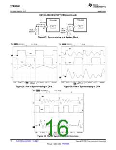
DETAILED DESCRIPTION (continued)
5.6
5.5
5.4
5.3
5.2
5.1
Dropout
Voltage
5
4.9
Dropout
4.8
Voltage
4.7
4.6
Start
0.35 0.4
Stop
0.45 0.5
0
0.05
0.1
0.15 0.2
0.25 0.3
Load Current - A
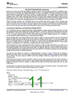
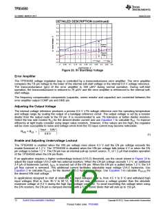
Figure 23. 5V Start/Stop Voltage
Error Amplifier
The TPS54560 voltage regulation loop is controlled by a transconductance error amplifier. The error amplifier
compares the FB pin voltage to the lower of the internal soft-start voltage or the internal 0.8 V voltage reference.
The transconductance (gm) of the error amplifier is 350 μA/V during normal operation. During soft-start
operation, the transconductance is reduced to 78 μA/V and the error amplifier is referenced to the internal soft-
start voltage.
The frequency compensation components (capacitor, series resistor and capacitor) are connected between the
error amplifier output COMP pin and GND pin.
Adjusting the Output Voltage
The internal voltage reference produces a precise 0.8 V ±1% voltage reference over the operating temperature
and voltage range by scaling the output of a bandgap reference circuit. The output voltage is set by a resistor
divider from the output node to the FB pin. It is recommended to use 1% tolerance or better divider resistors.
Select the low side resistor RLS for the desired divider current and use Equation 1 to calculate RHS. To improve
efficiency at light loads consider using larger value resistors. However, if the values are too high, the regulator
will be more susceptible to noise and voltage errors from the FB input current may become noticeable.
Vout - 0.8V
æ
ö
RHS = RLS
´
ç
÷
0.8 V
è
ø
(1)
Enable and Adjusting Undervoltage Lockout
The TPS54560 is enabled when the VIN pin voltage rises above 4.3 V and the EN pin voltage exceeds the
enable threshold of 1.2 V. The TPS54560 is disabled when the VIN pin voltage falls below 4 V or when the EN
pin voltage is below 1.2 V. The EN pin has an internal pull-up current source, I1, of 1.2 μA that enables operation
of the TPS54560 when the EN pin floats.
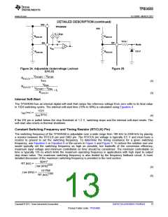
If an application requires a higher undervoltage lockout (UVLO) threshold, use the circuit shown in Figure 24 to
adjust the input voltage UVLO with two external resistors. When the EN pin voltage exceeds 1.2 V, an additional
3.4 μA of hysteresis current, IHYS, is sourced out of the EN pin. When the EN pin is pulled below 1.2 V, the 3.4
μA Ihys current is removed. This additional current facilitates adjustable input voltage UVLO hysteresis. Use
Equation 2 to calculate RUVLO1 for the desired UVLO hysteresis voltage. Use Equation 3 to calculate RUVLO2 for
the desired VIN start voltage.
In applications designed to start at relatively low input voltages (that is, from 4.5 V to 9 V) and withstand high
input voltages (that is, from 40 V to 60 V), the EN pin may experience a voltage greater than the absolute
maximum voltage of 8.4 V during the high input voltage condition. To avoid exceeding this voltage when using
the EN resistors, the EN pin is clamped internally with a 5.8 V zener diode that will sink up to 150 μA.
12
Submit Documentation Feedback
Copyright © 2013, Texas Instruments Incorporated
Product Folder Links: TPS54560

 TI [ TEXAS INSTRUMENTS ]