TPS54560
www.ti.com
SLVSBN0 –MARCH 2013
DETAILED DESCRIPTION (continued)
Overvoltage Protection
The TPS54560 incorporates an output overvoltage protection (OVP) circuit to minimize voltage overshoot when
recovering from output fault conditions or strong unload transients in designs with low output capacitance. For
example, when the power supply output is overloaded the error amplifier compares the actual output voltage to
the internal reference voltage. If the FB pin voltage is lower than the internal reference voltage for a considerable
time, the output of the error amplifier will increase to a maximum voltage corresponding to the peak current limit
threshold. When the overload condition is removed, the regulator output rises and the error amplifier output
transitions to the normal operating level. In some applications, the power supply output voltage can increase
faster than the response of the error amplifier output resulting in an output overshoot.
The OVP feature minimizes output overshoot when using a low value output capacitor by comparing the FB pin
voltage to the rising OVP threshold which is nominally 109% of the internal voltage reference. If the FB pin
voltage is greater than the rising OVP threshold, the high side MOSFET is immediately disabled to minimize
output overshoot. When the FB voltage drops below the falling OVP threshold which is nominally 106% of the
internal voltage reference, the high side MOSFET resumes normal operation.
Thermal Shutdown
The TPS54560 provides an internal thermal shutdown to protect the device when the junction temperature
exceeds 176°C. The high side MOSFET stops switching when the junction temperature exceeds the thermal trip
threshold. Once the die temperature falls below 164°C, the device reinitiates the power up sequence controlled
by the internal soft-start circuitry.
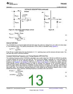
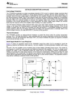
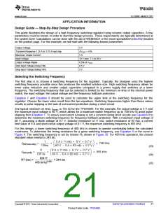
Small Signal Model for Loop Response
Figure 31 shows an equivalent model for the TPS54560 control loop which can be simulated to check the
frequency response and dynamic load response. The error amplifier is a transconductance amplifier with a gmEA
of
350 μA/V. The error amplifier can be modeled using an ideal voltage controlled current source. The resistor Ro
and capacitor Co model the open loop gain and frequency response of the amplifier. The 1mV ac voltage source
between the nodes a and b effectively breaks the control loop for the frequency response measurements.
Plotting c/a provides the small signal response of the frequency compensation. Plotting a/b provides the small
signal response of the overall loop. The dynamic loop response can be evaluated by replacing RL with a current
source with the appropriate load step amplitude and step rate in a time domain analysis. This equivalent model is
only valid for continuous conduction mode (CCM) operation.
SW
V
O
Power Stage
gm 17 A/V
ps
a
b
R
R1
ESR
R
COMP
L
c
FB
C
OUT
0.8 V
CO
RO
R3
C1
gm
ea
C2
R2
350 mA/V
Figure 31. Small Signal Model for Loop Response
Copyright © 2013, Texas Instruments Incorporated
Submit Documentation Feedback
17
Product Folder Links: TPS54560

 TI [ TEXAS INSTRUMENTS ]