TPS54560
www.ti.com
SLVSBN0 –MARCH 2013
DETAILED DESCRIPTION (continued)
When in Eco-mode, the COMP pin voltage is clamped at 600 mV and the high side MOSFET is inhibited. Since
the device is not switching, the output voltage begins to decay. The voltage control loop responds to the falling
output voltage by increasing the COMP pin voltage. The high side MOSFET is enabled and switching resumes
when the error amplifier lifts COMP above the pulse skipping threshold. The output voltage recovers to the
regulated value, and COMP eventually falls below the Eco-mode pulse skipping threshold at which time the
device again enters Eco-mode. The internal PLL remains operational when in Eco-mode. When operating at light
load currents in Eco-mode, the switching transitions occur synchronously with the external clock signal.
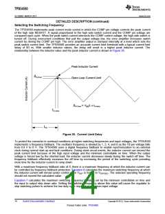
During Eco-mode operation, the TPS54560 senses and controls peak switch current, not the average load
current. Therefore the load current at which the device enters Eco-mode is dependent on the output inductor
value. The circuit in Figure 35 enters Eco-mode at about 25.3 mA output current. As the load current approaches
zero, the device enters a pulse skip mode during which it draws only 146 μA input quiescent current.
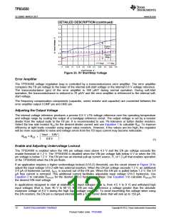
Low Dropout Operation and Bootstrap Voltage (BOOT)
The TPS54560 provides an integrated bootstrap voltage regulator. A small capacitor between the BOOT and SW
pins provides the gate drive voltage for the high side MOSFET. The BOOT capacitor is refreshed when the high
side MOSFET is off and the external low side diode conducts. The recommended value of the BOOT capacitor is
0.1 μF. A ceramic capacitor with an X7R or X5R grade dielectric with a voltage rating of 10 V or higher is
recommended for stable performance over temperature and voltage.
When operating with a low voltage difference from input to output, the high side MOSFET of the TPS54560 will
operate at 100% duty cycle as long as the BOOT to SW pin voltage is greater than 2.1V. When the voltage from
BOOT to SW drops below 2.1V, the high side MOSFET is turned off and an integrated low side MOSFET pulls
SW low to recharge the BOOT capacitor. To reduce the losses of the small low side MOSFET at high output
voltages, it is disabled at 24 V output and re-enabled when the output reaches 21.5 V.
Since the gate drive current sourced from the BOOT capacitor is small, the high side MOSFET can remain on for
many switching cycles before the MOSFET is turned off to refresh the capacitor. Thus the effective duty cycle of
the switching regulator can be high, approaching 100%. The effective duty cycle of the converter during dropout
is mainly influenced by the voltage drops across the power MOSFET, the inductor resistance, the low side diode
voltage and the printed circuit board resistance.
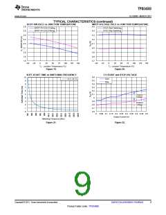
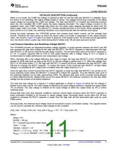
The start and stop voltage for a typical 5 V output application is shown in Figure 23 where the Vin voltage is
plotted versus load current. The start voltage is defined as the input voltage needed to regulate the output within
1% of nominal. The stop voltage is defined as the input voltage at which the output drops by 5% or where
switching stops.
During high duty cycle (low dropout) conditions, inductor current ripple increases when the BOOT capacitor is
being recharged resulting in an increase in output voltage ripple. Increased ripple occurs when the off time
required to recharge the BOOT capacitor is longer than the high side off time associated with cycle by cycle
PWM control.
At heavy loads, the minimum input voltage must be increased to insure a monotonic startup. The equation below
can be used to calculate the minimum input voltage for this condition.
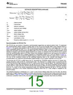
Vout_max = Dmax x (Vin_min - Iout_max x RDS(on) + VF) - VF + Iout_max x RL
Where:
Dmax ≥ 0.9
IB2SW = 100 µA
VF = Forward Drop of the Catch Diode
TSW = 1 / Fsw
VB2SW = VBOOT + VF
VBOOT = (1.41 x VIN - 0.554 - VF / TSW - 1.847 x 10³ x IB2SW) / (1.41 + 1 / Tsw)
RDS(on) = 1 / (-0.3 x VB2SW2 + 3.577 x VB2SW - 4.246)
spacer
Copyright © 2013, Texas Instruments Incorporated
Submit Documentation Feedback
11
Product Folder Links: TPS54560

 TI [ TEXAS INSTRUMENTS ]