TPS54560
SLVSBN0 –MARCH 2013
www.ti.com
OVERVIEW
The TPS54560 is a 60 V, 5 A, step-down (buck) regulator with an integrated high side n-channel MOSFET. The
device implements constant frequency, current mode control which reduces output capacitance and simplifies
external frequency compensation. The wide switching frequency range of 100 kHz to 2500 kHz allows either
efficiency or size optimization when selecting the output filter components. The switching frequency is adjusted
using a resistor to ground connected to the RT/CLK pin. The device has an internal phase-locked loop (PLL)
connected to the RT/CLK pin that will synchronize the power switch turn on to a falling edge of an external clock
signal.
The TPS54560 has a default input start-up voltage of approximately 4.3 V. The EN pin can be used to adjust the
input voltage undervoltage lockout (UVLO) threshold with two external resistors. An internal pull up current
source enables operation when the EN pin is floating. The operating current is 146 μA under no load condition
(not switching). When the device is disabled, the supply current is 2 μA.
The integrated 92mΩ high side MOSFET supports high efficiency power supply designs capable of delivering 5
amperes of continuous current to a load. The gate drive bias voltage for the integrated high side MOSFET is
supplied by a bootstrap capacitor connected from the BOOT to SW pins. The TPS54560 reduces the external
component count by integrating the bootstrap recharge diode. The BOOT pin capacitor voltage is monitored by a
UVLO circuit which turns off the high side MOSFET when the BOOT to SW voltage falls below a preset
threshold. An automatic BOOT capacitor recharge circuit allows the TPS54560 to operate at high duty cycles
approaching 100%. Therefore, the maximum output voltage is near the minimum input supply voltage of the
application. The minimum output voltage is the internal 0.8 V feedback reference.
Output overvoltage transients are minimized by an Overvoltage Transient Protection (OVP) comparator. When
the OVP comparator is activated, the high side MOSFET is turned off and remains off until the output voltage is
less than 106% of the desired output voltage.
The TPS54560 includes an internal soft-start circuit that slows the output rise time during start-up to reduce in-
rush current and output voltage overshoot. Output overload conditions reset the soft-start timer. When the
overload condition is removed, the soft-start circuit controls the recovery from the fault output level to the nominal
regulation voltage. A frequency foldback circuit reduces the switching frequency during start-up and overcurrent
fault conditions to help maintain control of the inductor current.
DETAILED DESCRIPTION
Fixed Frequency PWM Control
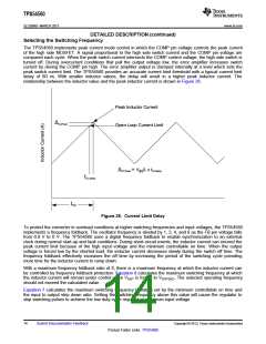
The TPS54560 uses fixed frequency, peak current mode control with adjustable switching frequency. The output
voltage is compared through external resistors connected to the FB pin to an internal voltage reference by an
error amplifier. An internal oscillator initiates the turn on of the high side power switch. The error amplifier output
at the COMP pin controls the high side power switch current. When the high side MOSFET switch current
reaches the threshold level set by the COMP voltage, the power switch is turned off. The COMP pin voltage will
increase and decrease as the output current increases and decreases. The device implements current limiting by
clamping the COMP pin voltage to a maximum level. The pulse skipping Eco-mode is implemented with a
minimum voltage clamp on the COMP pin.
Slope Compensation Output Current
The TPS54560 adds a compensating ramp to the MOSFET switch current sense signal. This slope
compensation prevents sub-harmonic oscillations at duty cycles greater than 50%. The peak current limit of the
high side switch is not affected by the slope compensation and remains constant over the full duty cycle range.
Pulse Skip Eco-mode
The TPS54560 operates in a pulse skipping Eco-mode at light load currents to improve efficiency by reducing
switching and gate drive losses. If the output voltage is within regulation and the peak switch current at the end
of any switching cycle is below the pulse skipping current threshold, the device enters Eco-mode. The pulse
skipping current threshold is the peak switch current level corresponding to a nominal COMP voltage of 600 mV.
10
Submit Documentation Feedback
Copyright © 2013, Texas Instruments Incorporated
Product Folder Links: TPS54560

 TI [ TEXAS INSTRUMENTS ]