TPS43060
TPS43061
SLVSBP4A –DECEMBER 2012–REVISED DECEMBER 2012
www.ti.com
æ
ö
÷
Qgd ´ RG
fSW
IOUT
2
ç
P
=
´ COSS ´VOUT +VOUT
´
´
SW
ç
è
÷
ø
2
1- Dmax VCC -VGS th
( )
ö
750kHz
2A
1.6nC ´1.2W
æ
=
´ 680pF ´15V 2 +15V ´
´
= 0.070W
ç
÷
2
1- 60% 5.5V -1.1V
è
ø
(27)
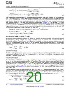
Two power losses in the high-side FET to consider are the dead time body diode loss and the FET conduction
loss. The conduction loss is highest at the minimum PWM duty cycle. The conduction power loss in the high-side
FET can be calculated with Equation 28. Dead time losses are caused by conduction in the body diode of the
high-side FET during the delay time between the LDRV and HDRV signals. The dead time loss varies mainly
with switching frequency. The dead time losses are estimated with Equation 29. The high-side FET of the
CSD86330Q3D has RDS(ON)HS = 8 mΩ and body diode forward voltage drop VSD = 0.75 V. The conduction power
losses are estimated at 0.080 W and the dead time losses are estimated at 0.366 W. For designs targeting
highest efficiency, dead time losses can be reduced by adding a Schottky diode in parallel with the high-side FET
to reduce the diode forward voltage drop during the dead time.
P
= 1- Dmax ´ I rms2 ´ R
= 1- 60% ´5.0A2 ´8mW = 0.080W
(
)
(
)
CONDHS
L
DS(on)LS
(28)
PDT = VSD ´ I rms ´ tnon-overlap1 + tnon-overlap2 ´ f
(
)
= 0.75V ´5A´ 60ns + 65ns ´750kHz = 0.366W
L
SW
(
)
(29)
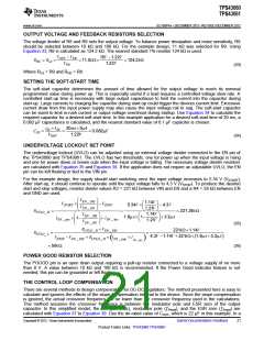
BOOTSTRAP CAPACITOR SELECTION
A capacitor must be connected between the BOOT and SW pins for proper operation. This capacitor provides
the instantaneous charge and gate drive voltage needed to turn on the high-side FET. A ceramic with X5R or
better grade dielectric is recommended. Use Equation 30 to calculate the minimum bootstrap capacitance to limit
the BOOT capacitor ripple voltage to 250 mV. In this example with the selected high-side FET the minimum
calculated capacitance is 0.042 µF and a 0.1 µF capacitor is used. The capacitor should have a 10 V or higher
voltage rating.
QgHS
5nC
CBOOT
=
=
DVBOOT 250mV
= 0.042mF
(30)
VCC CAPACITOR
An X5R or better grade ceramic bypass capacitor is required for the internal VCC regulator at the VCC pin with a
recommended range of 0.47 µF to 10 µF. A capacitance of 4.7 µF is used in this example. The capacitor should
have a 10 V or higher voltage rating.
INPUT CAPACITOR
The TPS43060 and TPS43061 require a high quality 0.1 µF or higher ceramic type X5R or X7R bypass capacitor
at the VIN pin for proper decoupling. Based on the application requirements additional bulk capacitance may be
needed to meet input voltage ripple and, or transient requirements. The minimum capacitance for a specified
input voltage ripple is calculated using Equation 31. The voltage rating of the input capacitor must be greater
than the maximum input voltage. The capacitor must also have a ripple current rating greater than the RMS
current calculated with Equation 32. If ceramic input capacitors are used they should be high quality ceramic,
type X5R or X7R.
For this example design, the capacitors must be rated for at least 12 V to support the maximum input voltage.
Designing for a 45 mV input voltage ripple (0.5% the nominal input voltage), the minimum input capacitance is
10.8 µF. The input capacitor must also be rated for 0.42 A RMS current. The capacitors selected are 2 x 10 µF,
25 V ceramic capacitors with 5 mΩ of ESR. The estimated voltage de-rated total capacitance is 15 µF.
IRIPPLE
1.46A
CIN
>
=
4´ fSW ´VINRIPPLE 4´ 750kHz ´ 0.045V
= 10.8mF
(31)
(32)
IRIPPLE
1.46A
ICIN rms =
=
= 0.42A
12
12
20
Submit Documentation Feedback
Copyright © 2012, Texas Instruments Incorporated
Product Folder Links: TPS43060 TPS43061

 TI [ TEXAS INSTRUMENTS ]