TPS43060
TPS43061
SLVSBP4A –DECEMBER 2012–REVISED DECEMBER 2012
www.ti.com
THERMAL CONSIDERATIONS
The maximum IC junction temperature should be restricted to 150°C under normal operating conditions. This
restriction limits the power dissipation of the TPS43060 and TPS43061. The devices are packaged in a thermally
enhanced QFN package which includes a PowerPAD™ that improves the thermal capabilities. The thermal
resistance of the QFN package in any application greatly depends on the PCB layout and the PowerPAD
connection. The PowerPAD must be soldered to the analog ground on the PCB. Use thermal vias underneath
the PowerPAD to achieve good thermal performance.
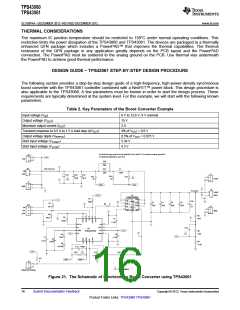
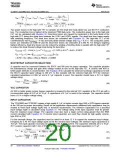
DESIGN GUIDE – TPS43061 STEP-BY-STEP DESIGN PROCEDURE
The following section provides a step-by-step design guide of a high-frequency, high-power-density synchronous
boost converter with the TPS43061 controller combined with a NexFET™ power block. This design procedure is
also applicable to the TPS43060. A few parameters must be known in order to start the design process. These
requirements are typically determined at the system level. For this example, we will start with the following known
parameters.
Table 2. Key Parameters of the Boost Converter Example
Input voltage (VIN
Output voltage (VOUT
Maximum output current (IOUT
Transient response to 0.5 A to 1.5 A load step (ΔVOUT
Output voltage ripple (VRIPPLE
Start input voltage (VSTART
Start input voltage (VSTOP
)
6 V to 12.6 V, 9 V nominal
)
15 V
)
2 A
)
4% of VOUT = 0.6 V
0.5% of VOUT = 0.075 V
5.34 V
)
)
)
4.3 V
Figure 21. The Schematic of Synchronous Boost Converter using TPS43061
16
Submit Documentation Feedback
Copyright © 2012, Texas Instruments Incorporated
Product Folder Links: TPS43060 TPS43061

 TI [ TEXAS INSTRUMENTS ]