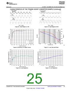
TPS43060
TPS43061
www.ti.com
SLVSBP4A –DECEMBER 2012–REVISED DECEMBER 2012
OUTPUT VOLTAGE AND FEEDBACK RESISTORS SELECTION
The voltage divider of R8 and R9 sets the output voltage. To balance power dissipation and noise sensitivity, R9
should be selected between 10 kΩ and 100 kΩ. For the example design, 11 kΩ was selected for R9. Using
Equation 33, R8 is calculated as 124.2 kΩ. The nearest standard 1% resistor 124 kΩ is used.
VOUT -VFB
15V -1.22V
RHS = RLS
´
= 11.0kW ´
= 124.2kW
VFB
1.22V
(33)
Where RLS = R9 and RHS = R8.
SETTING THE SOFT-START TIME
The soft-start capacitor determines the amount of time allowed for the output voltage to reach its nominal
programmed value during power up. This is especially useful if a load requires a controlled voltage slew rate. A
controlled start-up time is necessary with large output capacitance to limit the current into the capacitor during
start-up. Large currents to charging the capacitor during start-up could trigger the devices current limit. Excessive
current draw from the input power supply may also cause the input voltage rail to sag. The soft-start capacitor
can be sized to limit in-rush current or output voltage overshoot during startup. Use Equation 34 to calculate the
required capacitor for a desired soft-start time. In this example application for a desired soft-start time of 20 ms, a
0.082 µF capacitance is calculated, and the nearest standard value of 0.1 µF capacitor is chosen.
tSS ´ ISS
20ms ´5mA
CSS
=
=
= 0.082mF
VREF
1.22V
(34)
UNDERVOLTAGE LOCKOUT SET POINT
The undervoltage lockout (UVLO) can be adjusted using an external voltage divider connected to the EN pin of
the TPS43060 and TPS43061. The UVLO has two thresholds, one for power up when the input voltage is rising
and one for power down or brown outs when the input voltage is falling. The necessary voltage divider resistors
are calculated with Equation 35 and Equation 36. If the application does not require an adjustable UVLO, the EN
pin can be left floating or tied to the VIN pin.
For the example design, the supply should start switching once the input voltage increases to 5.34 V (VSTART).
After start-up, it should continue to operate until the input voltage falls to 4.3 V (VSTOP). To produce the desired
start and stop voltages, resistor divider values R3 = 221 kΩ between VIN and EN and a R4 = 59 kΩ between EN
and GND are used.
æ
ö
VEN _ DIS
1.14V
1.21V
1.14V
æ
ö
VSTART
´
-V
ç
ç
è
÷
÷
ø
STOP
5.34V ´
- 4.3V
ç
è
÷
VEN _ ON
ø
ö
RUVLO_ H
=
=
= 221.26kW
æ
ö
æ
VEN _ DIS
1.8mA´ 1-
+ 3.2mA
÷
ç
IEN _ pus ´ 1-
+ I
EN _ hys
ç
÷
÷
ø
1.21V
ç
è
è
ø
VEN _ ON
(35)
(36)
RUVLO_ H ´VEN _ DIS
221kW ´1.14V
4.3V -1.14V + 221kW ´ 1.8mA + 3.2mA
RUVLO_ L
=
=
(
)
VSTOP -VEN _ DIS + RUVLO _ H ´ I
(
+ I
)
EN _ pup
EN _ hys
POWER GOOD RESISTOR SELECTION
The PGOOD pin is an open drain output requiring a pull-up resistor connected to a voltage supply of no more
than 8 V. A value between 10 kΩ and 100 kΩ is recommended. If the Power Good indicator feature is not
needed, this pin can be grounded or left floating.
THE CONTROL LOOP COMPENSATION
There are several methods to design compensation for DC-DC regulators. The method presented here is easy to
calculate and ignores the effects of the slope compensation internal to the device. Since the slope compensation
is ignored, the actual crossover frequency will be lower than the crossover frequency used in the calculations.
This method assumes the crossover frequency is between the modulator pole and ESR zero of the output
capacitor. In this simplified model, the DC gain (Adc), modulator pole (ƒPmod), and the ESR zero (ƒZmod) are
calculated with Equation 37 to Equation 39. Use the de-rated value of COUT, which is 22 µF in this example. In a
Copyright © 2012, Texas Instruments Incorporated
Submit Documentation Feedback
21
Product Folder Links: TPS43060 TPS43061

 TI [ TEXAS INSTRUMENTS ]