TPS43060
TPS43061
SLVSBP4A –DECEMBER 2012–REVISED DECEMBER 2012
www.ti.com
THERMAL CONSIDERATIONS
The TPS43060 and TPS43061 junction temperature should not exceed 150°C under normal operating
conditions. This restriction limits the power dissipation of the device. Power dissipation of the controller includes
gate drive power loss and bias power loss of the internal VCC regulator. The TPS43060 and TPS43061 are
packaged in a thermally enhanced QFN package which includes a PowerPAD™ that improves the thermal
capabilities. The thermal resistance of the QFN package depends on the PCB layout and the PowerPAD
connection. As mentioned in the layout considerations, the PowerPAD must be soldered to the analog ground on
the PCB with thermal vias underneath the PowerPAD to achieve good thermal performance.
For best thermal performance pcb copper area should be sized to improve thermal capabilities of the
components in the power path dissipating the most power. This includes the sense resistors, inductor, low-side
FET and high-side FET. Manufacturer guidelines for the selected external FETs should be followed.
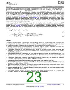
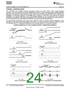
CHARACTERISTICS OF THE TPS43061 BOOST CONVERTER EXAMPLE
Vout (ac coupled)
200mV/div
VIN
5V/div
VCC
5V/div
VCC
5V/div
VOUT
Iout
5V/div
1A/div
PGOOD
5V/div
Time - 200 ms/div
Time – 5ms/div
Figure 22. Load Transient
Figure 23. Start-up with VIN
VOUT(ac coupled)
100mV/div
EN
5V/div
IL
1A/div
VCC
5V/div
Vout
SW
5V/div
10V/div
PGood
5V/div
Time - 5 ms/div
Time – 1µs/div
Figure 24. Start-up with EN
Figure 25. Output Ripple in CCM
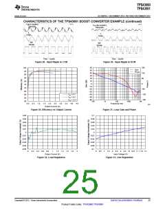
VOUT(ac coupled)
100mV/div
VOUT(ac coupled)
100mV/div
IL
IL
1A/div
1A/div
SW
SW
10V/div
10V/div
Time – 1µs/div
Time – 500µs/div
Figure 26. Output Ripple in DCM
Figure 27. Output Ripple in Pulse-Skipping Mode
24
Submit Documentation Feedback
Copyright © 2012, Texas Instruments Incorporated
Product Folder Links: TPS43060 TPS43061

 TI [ TEXAS INSTRUMENTS ]