TPS43060
TPS43061
www.ti.com
SLVSBP4A –DECEMBER 2012–REVISED DECEMBER 2012
SELECTING THE SWITCHING FREQUENCY
The first step is to determine the switching frequency of the power converter. There are tradeoffs to consider
when selecting a higher or lower switching frequency. Typically, the designer uses the highest switching
frequency possible since this results in the smallest solution size. A higher switching frequency allows for lower
value inductors and smaller output capacitors compared to a power converter that switches at a lower frequency.
A lower switching frequency will produce a larger solution size but typically has a better efficiency. Setting the
frequency for the minimum tolerable efficiency will produce the optimum solution size for the application.
The switching frequency can also be limited by the minimum on-time and off-time of the controller based on the
input voltage and the output voltage of the application. To determine the maximum allowable switching
frequency, first estimate the continuous conduction mode (CCM) duty cycle using Equation 11 with the minimum
and maximum input voltages. Equation 12 and Equation 13 should then be used to calculate the upper limit of
switching frequency for the regulator. Choose the lower value result from these two equations. Switching
frequencies higher than the calculated values will result in either pulse skipping if the minimum on-time restricts
the duty cycle or insufficient boost output voltage if the PWM duty cycle is limited by the minimum off-time.
VOUT - V
IN
D =
VOUT
(11)
Dmin
20%
fSW ontime =
=
= 2MHz
Dmin 60%
=
(12)
f
SW offtime =
= 2.4MHz
(13)
The typical minimum on-time and off-time of the device are 100 ns and 250 ns respectively. For this design, the
duty cycle is estimated at 20% and 60% with the maximum input voltage and minimum input voltage respectively.
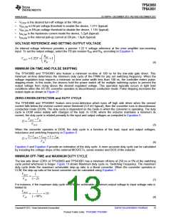
When operating at switching frequencies less than 200 kHz the minimum off time starts to increase and is equal
to 5% the switching period. The estimated allowed maximum switching frequency based on Equation 12 and
Equation 13 is 2 MHz. When operating near the estimated maximum duty cycle more accurate estimations of the
duty cycle should be made by including the voltage drops of the external MOSFETs, sense resistor and DCR of
the inductor.
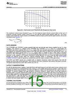
A switching frequency of 750 kHz is chosen as a compromise between efficiency and small solution size. To
determine the timing resistance for a given switching frequency use either Equation 14 or the curve in Figure 17.
The switching frequency is set by resistor R5 shown in Figure 21. For 750 kHz operation, the closest standard
value resistor is 76.8 kΩ.
57500
57500
RT (kW) =
=
fSW (kHz) 750(kHz)
= 76.7kW
(14)
INDUCTOR SELECTION
The selection of the inductor affects the steady-state operation as well as transient behavior and loop stability.
These factors make it an important component in a switching power supply design. The three most important
inductor specifications to consider are inductor value, DC resistance (DCR), and saturation current rating. Let the
parameter KIND represent the ratio of inductor peak-peak ripple current to the average inductor current. In a boost
topology the average inductor current is equal to the input current. The current delivered to the output is the input
current modulated at the duty cycle of the PWM. The inductor ripple current contributes to the output current
ripple that must be filtered by the output capacitor. Therefore, choosing high inductor ripple currents impacts the
selection of the output capacitor. The value of KIND in the design using low ESR output capacitors, such as
ceramics, can be relatively higher than that in the design using higher ESR output capacitors. Higher values of
KIND lead to discontinuous mode (DCM) operation at moderate to light loads.
To calculate the minimum value of the output inductor, use Equation 16 or Equation 17. In a boost topology
maximum current ripple occurs at 50% duty cycle. Use Equation 16 if the design will operate with 50% duty
cycle. If not, use Equation 17. In Equation 17, use the input voltage value that is nearest to 50% duty cycle
operation.
Copyright © 2012, Texas Instruments Incorporated
Submit Documentation Feedback
17
Product Folder Links: TPS43060 TPS43061

 TI [ TEXAS INSTRUMENTS ]