TPS43060
TPS43061
www.ti.com
SLVSBP4A –DECEMBER 2012–REVISED DECEMBER 2012
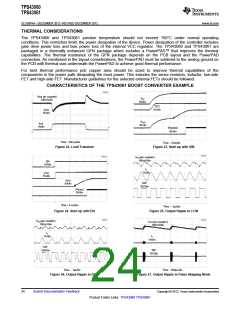
DISCONTINUOUS CONDUCTION MODE, PULSE-SKIP MODE AND NO LOAD INPUT CURRENT
The reverse current sensing of the TPS43060/61 allows the power supply to operate discontinuous conduction
mode (DCM) at light loads for higher efficiency. The supply enters DCM when the inductor current ramps to zero
at the end of a PWM cycle and the reverse current sense turns off the high-side FET for the remainder of the
cycle. In DCM the duty cycle is a function of the load, input and output voltages, inductance and switching
frequency as computed in Equation 47. The load current at which the inductor current falls to zero and the
converter enters DCM can be calculated using Equation 48. Additionally after the converter enters DCM,
decreasing the load further reduce the duty cycle. If the DCM on-time reaches the minimum on-time of the
TPS43060 and TPS43061, the converter begins pulse skipping to maintain output voltage regulation. Pulse
skipping can increase the output voltage ripple.
In this example with the 9 V nominal input voltage, the estimated load current where the converter enters DCM
operation is 0.44 A. The measured boundary is 0.36 A. In most designs the converter enters DCM at lower load
currents because Equation 48 does not account for the efficiency losses.. The design example power supply
enters pulse-skip mode when the output current is lower than 12 mA and the input current draw is 1.3 mA with
no load.
2´ V
(
-VIN ´ L ´ I
´ fSW
OUT
)
VIN
OUT
D =
(47)
(48)
2
V
(
-VIN ´V
)
15V - 9V ´ 9V 2
(
)
OUT
IN
IOUT crit =
=
= 0.44A
2´VOUT 2 ´ fSW ´ L 2´15V 2 ´ 750kHz ´ 3.3mH
LAYOUT
Layout is a critical portion of a good power converter design. There are several signal paths conducting fast
changing currents or voltages that can interact with stray inductance or parasitic capacitance to generate noise
or degrade performance. Guidelines are as follows and the EVM layouts can be used as reference.
•
The high speed switching current path includes the high-side FET, low-side FET and output capacitors. This
is a critical loop to minimize to reduce noise and achieve best performance.
•
Components connected to noise sensitive circuitry should be located as close to the TPS43060 and
TPS43061 as possible, and be connected the AGND pin. This includes components connected to FB, COMP,
SS, RT/CLK, and VCC pins.
•
•
The PowerPAD should be connected to the quiet analog ground for the AGND pin to limit internal noise. For
thermal performance, multiple vias directly under the device should be used to connect to any internal ground
planes.
Components in the power conversion path should be connected to the PGND. This includes the bulk input
capacitors, output capacitors, low-side FET and EN UVLO resistors.
•
•
A single connection must connect the quiet AGND to the noisy PGND near the PGND pin.
The low ESR ceramic bypass capacitor for the VIN pin should be connected to the quiet AGND as close as
possible to the TPS43060 and TPS43061.
•
•
•
The distance between the inductor, low-side FET and high-side FET should be minimized to reduce noise.
This connection is the high speed switching voltage node.
The high-side and low-side FETs should be placed close to the device to limit the trace length required for the
HDRV and LDRV gate drive signals.
The bypass capacitor between the ISNS+ and ISNS- pins should be placed next to the TPS43060 and
TPS43061. Minimize the distance between the device and the sense resistors.
Copyright © 2012, Texas Instruments Incorporated
Submit Documentation Feedback
23
Product Folder Links: TPS43060 TPS43061

 TI [ TEXAS INSTRUMENTS ]