TPS43060
TPS43061
www.ti.com
SLVSBP4A –DECEMBER 2012–REVISED DECEMBER 2012
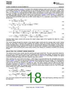
OUTPUT CAPACITOR SELECTION
In a boost topology the current supplied to the output capacitor is discontinuous and proper selection of the
output capacitor is important for filtering the high di/dt path of the supply. There are two primary considerations
for selecting the value of the output capacitor. The output capacitor determines the output voltage ripple, and
how the supply responds to a large change in load current. The output capacitance needs to be selected based
on the more stringent of these two criteria.
The desired response to a large change in load current is the first criteria. A PWM controller cannot immediately
respond to a fast increase or decrease in the load current. The response time is determined by the loop
bandwidth. The output capacitor must supply the increased load current or absorb the excess inductor current
until the controller responds. Equation 23 estimates the minimum output capacitance needed for the desired
ΔVOUT for a given ΔIOUT. The loop bandwidth (ƒBW) is typically limited by the Right Half Plane Zero (RHPZ) of the
boost topology. The maximum recommended bandwidth can be calculated from Equation 41 and Equation 42.
See the compensation section for more information. In this example, to limit the voltage deviation to 600 mV from
a 1 A load step with a 14.5 kHz maximum bandwidth, a minimum of 18.3 µF output capacitance is needed. This
value does not take into account the ESR of the output capacitor which can typically be ignored when using
ceramic capacitors.
The output capacitor absorbs the ripple current through the synchronous switch to limit the output voltage ripple.
Equation 24 calculates the minimum output capacitance needed to meet the output voltage ripple specification.
In this example, a minimum of 21.3 µF is needed. Again this value does not take into account the ESR of the
output capacitor.
DITRAN
2p´ fBW ´ DVTRAN 2p´14.5kHz ´ 0.6V
Dmax´ IOUT
1A
COUT
>
=
= 18.3mF
(23)
60%´5A
fSW ´VRIPPLE 750kHz ´ 0.075V
COUT
>
=
= 21.3mF
(24)
The most stringent criteria for the output capacitor is 21.3 µF required to limit the output voltage ripple. When
using ceramic capacitors for switching power supplies, high quality type X5R or X7R are recommended. They
have a high capacitance to volume ratio and are fairly stable over temperature. Capacitance de-ratings for aging,
temperature and dc bias increase the minimum value required. The voltage rating must be greater than the
output voltage with some tolerance for output voltage ripple and overshoot in transient conditions. For this
example 4 x 10 µF, 25 V ceramic capacitors with 5 mΩ of ESR are used. The estimated derated capacitance is
22 µF, approximately equal to the calculated minimum.
MOSFET SELECTION - NexFET™ POWER BLOCK
The TPS43061 5.5V gate drive is optimized for low Qg NexFET power devices. NexFET power blocks with both
the high-side and low-side MOSFETs integrated are ideal for high power density designs. This design example
uses the CSD86330Q3D. Two primary considerations when selecting the power MOSFETs are the average gate
drive current required and the estimated MOSFET power losses.
The average gate drive current must be less than the 50 mA (minimum) VCC supply current limit. This current is
calculated using Equation 25. With the selected power block and 5.5V VCC, the low-side FET has a total gate
charge of 11 nC and the high-side FET has a total gate charge of 5 nC. The required gate drive current is 12
mA.
IGD = (QgHS + QgLS )´ fSW = (5nC +11nC)´750kHz = 12mA
(25)
The target efficiency of the design dictates the acceptable power loss in the MOSFETs. The two largest
components of power loss in the low-side FET are switching and conduction losses. Both losses are highest at
the minimum input voltage when low-side FET current is maximum. The conduction power loss in the low-side
FET can be calculated with Equation 26. Switching losses occur during the turn-off and turn-on time of the
MOSFET. During these transitions, the low-side FET experiences both the input current and output voltage. The
switching loss can be estimated with Equation 27. The low-side FET of the CSD86330Q3D has RDS(on)LS = 4.2
mΩ, gate to drain charge Qgd = 1.6 nC, output capacitance COSS = 680 pF, series gate resistance RG = 1.2 Ω,
and gate to source voltage threshold VGS(th) = 1.1 V. The conduction power losses are estimated at 0.042 W and
the switching losses are estimated at 0.070 W.
P
= Dmax´ ILrms2 ´ RdsonLS = 60%´5.0A2 ´ 4.2mW = 0.042W
CONDLS
(26)
Copyright © 2012, Texas Instruments Incorporated
Submit Documentation Feedback
19
Product Folder Links: TPS43060 TPS43061

 TI [ TEXAS INSTRUMENTS ]