TPS43060
TPS43061
www.ti.com
SLVSBP4A –DECEMBER 2012–REVISED DECEMBER 2012
78
74
70
66
62
58
54
50
0
10
20
30
40
50
60
70
80
90 100
C020
Duty Cycle (%)
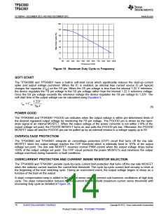
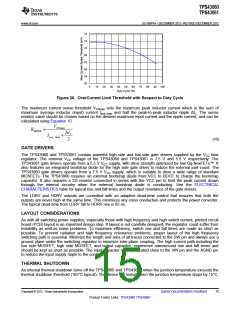
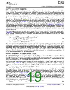
Figure 20. OverCurrent Limit Threshold with Respect to Duty Cycle
The maximum current sense threshold VCSmax sets the maximum peak inductor current which is the sum of
maximum average inductor (input) current Iave_max and half the peak-to-peak inductor ripple ΔIL. The sense
resistor value should be chosen based on the desired maximum input current and the ripple current, and can be
calculated using Equation 10.
VCS max
RSENSE
=
DIL
Iave_ max
+
(10)
GATE DRIVERS
The TPS43060 and TPS43061 contain powerful high-side and low-side gate drivers supplied by the VCC bias
regulator. The nominal VCC voltage of the TPS43060 and TPS43061 is 7.5 V and 5.5 V respectively. The
TPS43061 gate drivers operate from a 5.5 V VCC supply, with drive strength optimized for low Qg NexFETs™. It
also features an integrated bootstrap diode for the high side gate driver to reduce the external part count. The
TPS43060 gate drivers operate from a 7.5 V VCC supply, which is suitable to drive a wide range of standard
MOSFETs. The TPS43060 requires an external bootstrap diode from VCC to BOOT to charge the bootstrap
capacitor. It also requires a 2Ω resistor connected in series with the VCC pin to limit the peak current drawn
through the internal circuitry when the external bootstrap diode is conducting. See the ELECTRICAL
CHARACTERISTICS table for typical rise and fall times and the output resistance of the gate drivers.
The LDRV and HDRV outputs are controlled with an adaptive dead-time control that ensures that both the
outputs are never high at the same time. This minimizes any cross conduction and protects the power converter.
The typical dead-time from LDRV fall to HDRV rise is 65 ns.
LAYOUT CONSIDERATIONS
As with all switching power supplies, especially those with high frequency and high switch current, printed circuit
board (PCB) layout is an important design step. If layout is not carefully designed, the regulator could suffer from
instability as well as noise problems. To maximize efficiency, switch rise and fall times are made as short as
possible. To prevent radiation and high frequency resonance problems, proper layout of the high frequency
switching path is essential. Minimize the length and area of all traces connected to the SW pin and always use a
ground plane under the switching regulator to minimize inter-plane coupling. The high current path including the
low side MOSFET, high side MOSFET, and output capacitor, experience nanosecond rise and fall times and
should be kept as short as possible. The input capacitor must be located close to the VIN pin and the AGND pin
to reduce the input supply ripple to the controller.
THERMAL SHUTDOWN
An internal thermal shutdown turns off the TPS43060 and TPS43061 when the junction temperature exceeds the
thermal shutdown threshold (165°C typical). The device will restart when the junction temperature drops by 15°C.
Copyright © 2012, Texas Instruments Incorporated
Submit Documentation Feedback
15
Product Folder Links: TPS43060 TPS43061

 TI [ TEXAS INSTRUMENTS ]