TPS40210-Q1, TPS40211-Q1
SLVS861D –AUGUST 2008–REVISED APRIL 2010
www.ti.com
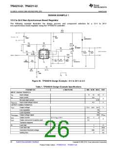
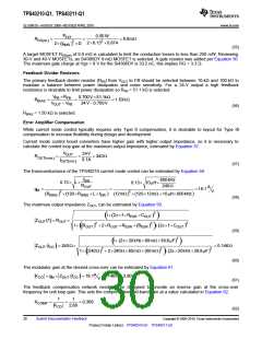
DESIGN EXAMPLE 1
12-V to 24-V Non-Synchronous Boost Regulator
The following example illustrates the design process and component selection for a 12-V to 24-V
non-synchronous boost regulator using the TPS40210 controller.
+
+
Figure 30. TPS40210 Design Example – 8-V to 24-V at 2-A
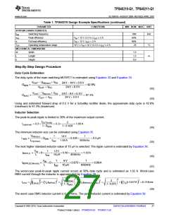
Table 1. TPS40210 Design Example Specifications
PARAMETER
INPUT CHARACTERISTICS
CONDITIONS
MIN NOM MAX UNIT
VIN
IIN
Input voltage
8
12
14
V
A
V
Input current
4.4
No load input current
Input undervoltage lockout
0.05
VIN(UVLO)
4.5
OUTPUT CHARACTERISTICS
VOUT
Output voltage
Line regulation
Load regulation
23.5 24.0 24.5
V
1%
1%
VOUT(ripple) Output voltage ripple
500 mVPP
IOUT
IOCP
Output current
8 V ≤ VIN ≤ 14 V
0.2
3.5
1
2
A
Output overcurrent inception point
Transient response
Load step
ΔI
1
1
A
Load slew rate
A/ms
mV
ms
Overshoot threshold voltage
Settling time
500
5
26
Submit Documentation Feedback
Copyright © 2008–2010, Texas Instruments Incorporated
Product Folder Link(s): TPS40210-Q1 TPS40211-Q1

 TI [ TEXAS INSTRUMENTS ]