TPS40210-Q1, TPS40211-Q1
www.ti.com
SLVS861D –AUGUST 2008–REVISED APRIL 2010
The error amplifier GBWP will usually be higher, but is ensured by design to be at least 1.5 MHz. If the gain
required in Equation 25 multiplied by 10 times the desired control loop crossover frequency, the high-frequency
pole introduced by CHF is overridden by the error amplifier capability and the effective pole is lower in frequency.
If this is the case, CHF can be made larger to provide a consistent high-frequency roll off in the control loop
design. Equation 29 calculates the required CHF in this case.
1
CHF
=
2p´1.5´ 10 6 ´RFB
( )
where
•
•
CHF is the high-frequency roll-off capacitor value in mF
RFB is the mid-band gain-setting resistor value in Ω
(29)
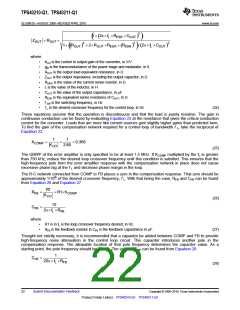
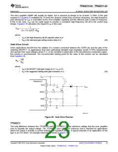
Gate Drive Circuit
Some applications benefit from the addition of a resistor connected between the GDRV pin and the gate of the
switching MOSFET. In applications that have particularly stringent load regulation (under 0.75%) requirements
and operate from input voltages above 5 V, or are sensitive to pulse jitter in the discontinuous conduction region,
this resistor is recommended. The recommended starting point for the value of this resistor can be calculated
from Equation 30.
105
=
R
G
Q
G
where
•
•
QG is the MOSFET total gate charge at 8-V VGS in nC.
RG is the suggested starting point gate resistance in Ω.
(30)
V
IN
TPS40210/11
VDD 10
L
V
OUT
R
G
GDRV
ISNS
GND
8
7
6
UDG-07196
Figure 28. Gate Drive Resistor
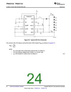
TPS40211
The only difference between the TPS40210 and the TPS40211 is the reference voltage that the error amplifier
uses to regulate the output voltage. The TPS40211 uses a 260-mV reference and is intended for applications
where the output is actually a current instead of a regulated voltage. A typical example of an application of this
type is an LED driver. An example schematic is shown in Figure 29.
Copyright © 2008–2010, Texas Instruments Incorporated
Submit Documentation Feedback
23
Product Folder Link(s): TPS40210-Q1 TPS40211-Q1

 TI [ TEXAS INSTRUMENTS ]