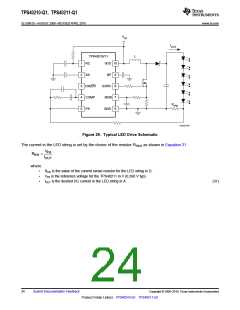
TPS40210-Q1, TPS40211-Q1
SLVS861D –AUGUST 2008–REVISED APRIL 2010
www.ti.com
2
1+ 2p´ f ´RESR ´ COUT
(
)
L
(
+ 2´ROUT ´RESR + R
)
´ 2p´ f ´C
ZOUT = ROUT
´
2
2
ESR ) (
2
1+
R
(
)
(
)
OUT
L OUT
(
)
where
•
•
•
•
•
•
•
•
•
•
KCO is the control to output gain of the converter, in V/V
gM is the transconductance of the power stage and modulator, in S
ROUT is the output load equivalent resistance, in Ω
ZOUT is the output impedance, including the output capacitor, in Ω
RISNS is the value of the current sense resistor, in Ω
L is the value of the inductor, in H
COUT is the value of the output capacitance, in mF
RESR is the equivalent series resistance of COUT, in Ω
f SW is the switching frequency, in Hz
f L is the desired crossover frequency for the control loop, in Hz
(24)
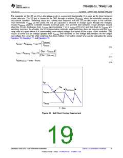
These equations assume that the operation is discontinuous and that the load is purely resistive. The gain in
continuous conduction can be found by evaluating Equation 23 at the resistance that gives the critical conduction
current for the converter. Loads that are more like current sources give slightly higher gains than predicted here.
To find the gain of the compensation network required for a control loop of bandwidth f , take the reciprocal of
L
Equation 22.
1
1
KCOMP
=
=
= 0.356
KCO
2.80
(25)
The GBWP of the error amplifier is only specified to be at least 1.5 MHz. If KCOMP multiplied by the fL is greater
than 750 kHz, reduce the desired loop crossover frequency until this condition is satisfied. This ensures that the
high-frequency pole from the error amplifier response with the compensation network in place does not cause
excessive phase lag at the f L and decrease phase margin in the loop.
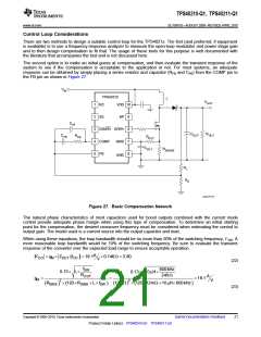
The R-C network connected from COMP to FB places a zero in the compensation response. That zero should be
approximately 1/10th of the desired crossover frequency, f . With that being the case, RFB and CFB can be found
L
from Equation 26 and Equation 27
R1
RFB
=
= R1´KCOMP
KCO
(26)
10
2p´ f ´R
C
=
FB
L
FB
where
•
•
R1 is in fL is the loop crossover frequency desired, in Hz.
RFB is the feedback resistor in CFB is the feedback capacitance in mF.
(27)
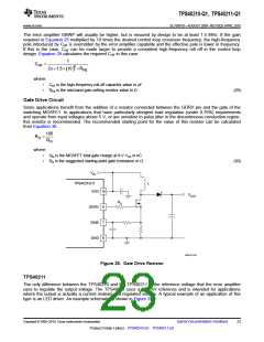
Thought not strictly necessary, it is recommended that a capacitor be added between COMP and FB to provide
high-frequency noise attenuation in the control loop circuit. This capacitor introduces another pole in the
compensation response. The allowable location of that pole frequency determines the capacitor value. As a
starting point, the pole frequency should be 10 × fL. The value of CHF can be found from Equation 28.
1
C
=
HF
20p´ f ´R
L
FB
(28)
22
Submit Documentation Feedback
Copyright © 2008–2010, Texas Instruments Incorporated
Product Folder Link(s): TPS40210-Q1 TPS40211-Q1

 TI [ TEXAS INSTRUMENTS ]