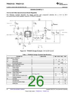
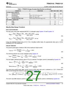
TPS40210-Q1, TPS40211-Q1
SLVS861D –AUGUST 2008–REVISED APRIL 2010
www.ti.com
P
0.50W
FET
RDS on
<
=
= 9.8mW
( )
2´ 6.132 ´0.674
2´ I
(
2 ´D
)
RMS
(55)
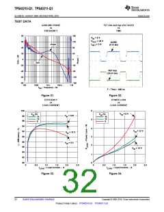
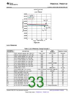
A target MOSFET RDS(on) of 9.8 mΩ is calculated to limit the conduction losses to less than 250 mW. Reviewing
30-V and 40-V MOSFETs, an Si4386DY 9-mΩ MOSFET is selected. A gate resistor was added per Equation 30.
The maximum gate charge at Vgs = 8 V for the Si4386DY is 33.2 nC, this implies RG = 3.3 Ω.
Feedback Divider Resistors
The primary feedback divider resistor (RFB) from VOUT to FB should be selected between 10-kΩ and 100-kΩ to
maintain a balance between power dissipation and noise sensitivity. For a 24-V output a high feedback
resistance is desirable to limit power dissipation so RFB = 51.1 kΩ is selected.
V
´R
FB
0.700V ´51.1kW
24V - 0.700V
FB
R
=
=
= 1.53kW
BIAS
V
- V
FB
OUT
(56)
RBIAS = 1.50 kΩ is selected.
Error Amplifier Compensation
While current mode control typically requires only Type II compensation, it is desirable to layout for Type III
compensation to increase flexibility during design and development.
Current mode control boost converters have higher gain with higher output impedance, so it is necessary to
calculate the control loop gain at the maximum output impedance, estimated by Equation 57.
VOUT
24V
0.1A
ROUT max
=
=
= 240W
(
)
IOUT min
(
)
(57)
(58)
(59)
The transconductance of the TPS40210 current mode control can be estimated by Equation 58.
fSW
600kHz
0.13´ L ´
2 ´ 120´R
0.13´ 10mH´
ROUT
240W
A
gM
=
=
(
)
= 19.1
12mW 2 ´ 120´12mW +10mH´ 600kHz
V
R
(
+ L ´ fSW
) (
)
ISNS ) (
ISNS
The maximum output impedance ZOUT, can be estimated by Equation 59.
2
1+ 2p´ f ´RESR ´ COUT
(
)
(
)
ZOUT(f ) = ROUT
´
2
)
2
ESR ) (
2
)
1+
R
+ 2´ROUT ´RESR + R
´ 2p´ f ´C
(
(
OUT
OUT
(
)
2
1+ 2p´ 20kHz ´ 60mW ´ 39.8mF
(
)
(
)
1+ 240W + 2´ 240W ´ 60mW + 60mW ´ 2p´ 20kHz ´39.8mF
ZOUT
f
(CO )
= 240W´
= 0.146W
2
)
2
)
2
) (
(
(
(
)
(60)
The modulator gain at the desired cross-over can be estimated by Equation 61.
A
KCO = gM ´ ZOUT
f
(CO )
= 19.1
´0.146W = 2.80
V
(61)
The feedback compensation network needs to be designed to provide an inverse gain at the cross-over
frequency for unit loop gain. This sets the compensation mid-band gain at a value calculated in Equation 62.
1
1
KCOMP
=
=
= 0.356
KCO
2.80
(62)
30
Submit Documentation Feedback
Copyright © 2008–2010, Texas Instruments Incorporated
Product Folder Link(s): TPS40210-Q1 TPS40211-Q1

 TI [ TEXAS INSTRUMENTS ]