TPS40210-Q1, TPS40211-Q1
SLVS861D –AUGUST 2008–REVISED APRIL 2010
www.ti.com
I
2
OUT(max)
1
1
I
»
+
I
( 2)RIPPLE(Vinmin)
=
+
0.718 = 6.57A
( 2)
Lpeak
1- D
1- 0.673
MAX
(39)
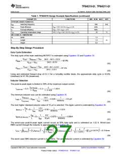
A 10-mH inductor with a minimum RMS current rating of 6.13 A and minimum saturation current rating of 6.57 A
must be selected. A TDK RLF12560T-100M-7R5 7.5-A 10-mH inductor is selected.
This inductor power dissipation is estimated by Equation 40.
P » I
(
2 ´DCR
Lrms
)
L
(40)
The TDK RLF12560T-100M-7R5 12.4-mΩ DCR dissipates 466 mW of power.
Rectifier Diode Selection
A low-forward voltage drop Schottky diode is used as a rectifier diode to reduce its power dissipation and
improve efficiency. Using 80% derating, on VOUT for ringing on the switch node, the rectifier diode minimum
reverse break-down voltage is given by Equation 41.
V
OUT
V
³
= 1.25´ V
= 1.25´ 24V = 30V
(BR)R(min)
OUT
0.8
(41)
The diode must have reverse breakdown voltage greater than 30 V. The rectifier diode peak and average
currents are estimated by Equation 42 and Equation 43.
ID avg » IOUT max = 2 A
(
)
(
)
(42)
(43)
ID peak = IL peak = 6.57A
(
)
(
)
For this design, 2-A average and 6.57-A peak is
The power dissipation in the diode is estimated by Equation 44.
P
» V ´I
= 0.5V ´ 2A = 1W
D(max)
F
OUT(max)
(44)
For this design, the maximum power dissipation is estimated as 1 W. Reviewing 30-V and 40-V Schottky diodes,
the MBRS340T3 40-V 3-A diode in an SMC package is selected. This diode has a forward voltage drop of 0.48 V
at 6 A, so the conduction power dissipation is approximately 960 mW, less than half its rated power dissipation.
Output Capacitor Selection
Output capacitors must be selected to meet the required output ripple and transient specifications.
IOUT ´D
æ
ç
è
ö
÷
ø
1
2A ´0.673
500mV
1
COUT = 8
´
= 8
´
= 35mF
VOUT(ripple) fSW
600kHz
(45)
(46)
VOUT ripple
7
(
)
7
500mV
ESR =
´
=
´
= 95mW
8
IL peak -IOUT
8
6.57A - 2A
(
)
A Panasonic EEEFC1V330P 35-V 33-mF, 120-mΩ bulk capacitor and 6.8-mF ceramic capacitor is selected to
provide the required capacitance and ESR at the switching frequency. The combined capacitances of 39.8 mF
and 60 mΩ are used in compensation calculations.
Input Capacitor Selection
Since a boost converter has continuous input current, the input capacitor senses only the inductor ripple current.
The input capacitor value can be calculated by Equation 47 and Equation 48 .
28
Submit Documentation Feedback
Copyright © 2008–2010, Texas Instruments Incorporated
Product Folder Link(s): TPS40210-Q1 TPS40211-Q1

 TI [ TEXAS INSTRUMENTS ]