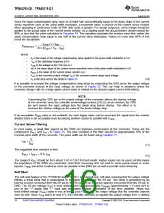
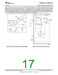
TPS40210-Q1, TPS40211-Q1
SLVS861D –AUGUST 2008–REVISED APRIL 2010
www.ti.com
BP Regulator
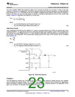
The TPS40210 and TPS40211 have an on-board linear regulator that supplies power for the internal circuitry of
the controller, including the gate driver. This regulator has a nominal output voltage of 8 V and must be bypassed
with a 1-mF capacitor. If the voltage at the VDD pin is less than 8 V, the voltage on the BP pin is also less, and
the gate drive voltage to the external FET is reduced from the nominal 8 V. This should be considered when
choosing a FET for the converter.
Connecting external loads to this regulator can be done, but care must be taken to ensure that the thermal rating
of the device is observed, because there is no thermal shutdown feature in this controller. Exceeding the thermal
ratings causes out-of-specification behavior and can lead to reduced reliability. The controller dissipates more
power when there is an external load on the BP pin and is tested for dropout voltage for up to 5-mA load. When
the controller is in the disabled state, the BP pin regulator also shuts off so loads connected there power down
as well. When the controller is disabled with the DIS/EN pin, this regulator is turned off.
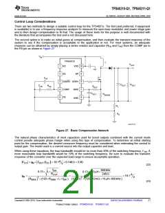
The total power dissipation in the controller can be calculated as follows. The total power is the sum of PQ, PG
and PE.
P
= V
´I
Q
VDD VDD(en)
(19)
(20)
P
= V
´ Q ´ f
SW
G
VDD
g
P = V
´I
E
VDD EXT
where
•
•
•
•
•
•
•
•
PQ is the quiescent power of the device in W
VVDD is the VDD pin voltage in V
IVDD(en) is the quiescent current of the controller when enabled but not switching in A
PG is the power dissipated by driving the gate of the FET in W
Qg is the total gate charge of the FET at the voltage on the BP pin in C
f SW is the switching frequency in Hz
PE is the dissipation caused be external loading of the BP pin in W
IEXT is the external load current in A
(21)
Shutdown (DIS/EN Pin)
The DIS/EN pin is an active-high shutdown command for the controller. Pulling this pin above 1.2 V causes the
controller to completely shut down and enter a low current consumption state. In this state, the regulator
connected to the BP pin is turned off. There is an internal 1.1-MΩ pull-down resistor connected to this pin that
keeps the pin at GND level when left floating. If this function is not used in an application, it is best to connect
this pin to GND
20
Submit Documentation Feedback
Copyright © 2008–2010, Texas Instruments Incorporated
Product Folder Link(s): TPS40210-Q1 TPS40211-Q1

 TI [ TEXAS INSTRUMENTS ]