TPS40210-Q1, TPS40211-Q1
SLVS861D –AUGUST 2008–REVISED APRIL 2010
www.ti.com
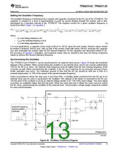
Since the slope compensation ramp must be at least half, and preferably equal to the down slope of the current
sense waveform seen at the pulse-width modulator, a maximum value is placed on the current sense resistor
when operating in continuous mode at 50% duty cycle or greater. For design purposes, some margin should be
applied to the actual value of the current sense resistor. As a starting point, the actual resistor chosen should be
80% or less that the value calculated in Equation 10. This equation calculates the resistor value that makes the
slope compensation ramp equal to one half of the current ramp downslope. Values no more than 80% of this
result are acceptable.
V
VDD ´L ´ fSW
RISNS(max)
=
60´ V + VD - V
(
)
OUT
IN
where
•
•
•
•
•
•
•
Se is the slope of the voltage compensating ramp applied to the pulse-width modulator in V/s
f SW is the switching frequency in Hz
VVDD is the voltage at the VDD pin in V
m2 is the down slope of the current sense waveform seen at the pulse-width modulator in V/s
RISNS is the value of the current sense resistor in Ω
VOUT is the converter output voltage VIN is the converter power stage input voltage
VD is the drop across the diode in Figure 23
(10)
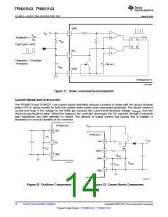
It is possible to increase the voltage compensation ramp slope by connecting the VDD pin to the output voltage
of the converter instead of the input voltage as shown in Figure 23. This can help in situations where the
converter design calls for a large ripple current value in relation to the desired output current limit setting.
NOTE
Connecting the VDD pin to the output voltage of the converter affects the startup voltage
of the converter since the controller undervoltage lockout (UVLO) circuit monitors the VDD
pin and senses the input voltage less the diode drop before startup. The effect is to
increase the startup voltage by the value of the diode voltage drop.
If an acceptable RISNS value is not available, the next higher value can be used and the signal from the resistor
divided down to an acceptable level by placing another resistor in parallel with CISNS
.
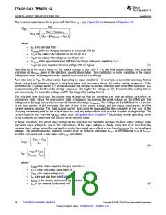
Current Sense Filtering
In most cases, a small filter placed on the ISNS pin improves performance of the converter. These are the
components RIFLT and CIFLT in Figure 23. The time constant of this filter should be approximately 10% of the
nominal pulse width of the converter. The pulse width can be found using Equation 11.
D
=
t
ON
f
SW
(11)
The suggested time constant is then
´ C = 0.1´ t
R
IFLT
IFLT
ON
(12)
The range of RIFLT should be from about 1 kΩ to 5 kΩ for best results. Higher values can be used, but this raises
the impedance of the ISNS pin connection more than necessary and can lead to noise-pickup issues in some
layouts. CISNS should be located as close as possible to the ISNS pin as well to provide noise immunity.
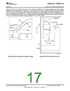
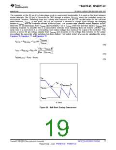
Soft Start
The soft-start feature of the TPS40210 and TPS40211 is a closed-loop soft start, meaning that the output voltage
follows a linear ramp that is proportional to the ramp generated at the SS pin. This ramp is generated by an
internal resistor connected from the BP pin to the SS pin and an external capacitor connected from the SS pin to
GND. The SS pin voltage (VSS) is level shifted down by approximately VSS(ofst) (approximately 1 V) and sent to
one of the “+” inputs (the “+” input with the lowest voltage dominates) of the error amplifier. When this
level-shifted voltage (VSSE) starts to rise at time t1 (see Figure 24), the output voltage that the controller expects
rises as well. Since VSSE starts at near 0 V, the controller attempts to regulate the output voltage from a starting
16
Submit Documentation Feedback
Copyright © 2008–2010, Texas Instruments Incorporated
Product Folder Link(s): TPS40210-Q1 TPS40211-Q1

 TI [ TEXAS INSTRUMENTS ]