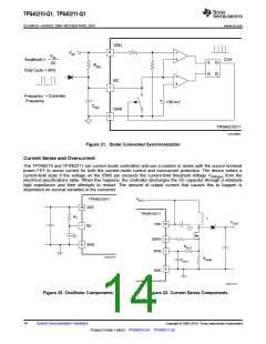
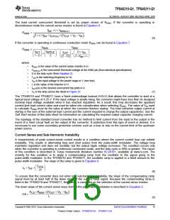
TPS40210-Q1, TPS40211-Q1
SLVS861D –AUGUST 2008–REVISED APRIL 2010
www.ti.com
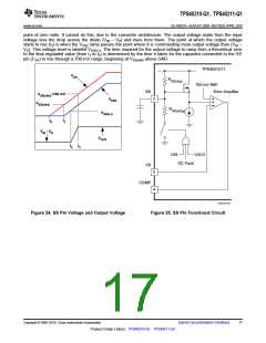
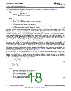
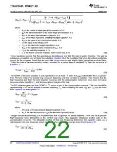
The required capacitance for a given soft start time t3 – t1 in Figure 24 is calculated in Equation 13.
t
SS
C
=
SS
æ
ç
ç
è
ö
÷
÷
V
- V
SS(ofst)
BP
R
´ln
SS
V
- V
+ V
(
)
BP
SS(ofst) FB
ø
where
•
•
•
•
•
•
tSS is the soft-start time
RSS(chg) is the SS charging resistance in Ω, typically 500 kΩ
CSS is the value of the capacitor on the SS pin, in F
VBP is the value of the voltage on the BP pin in V
VSS(ofst) is the approximate level shift from the SS pin to the error amplifier (~1 V)
VFB is the error amplifier reference voltage, 700 mV typical
(13)
Note that tSS is the time it takes for the output voltage to rise from 0 V to the final output voltage. Also note the
tolerance on RSS(chg) given in the electrical specifications table. This contributes to some variability in the output
voltage rise time, and margin must be applied to account for it in design.
Also take note of VBP. Its value varies depending on input conditions. For example, a converter operating from a
slowly rising input initializes VBP at a fairly low value and increases during the entire startup sequence. If the
controller has a voltage above 8 V at the input and the DIS pin is used to stop and then restart the converter, VBP
is approximately 8 V for the entire startup sequence. The higher the voltage on BP, the shorter the startup time is
and conversely, the lower the voltage on BP, the longer the startup time is.
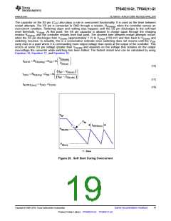
The soft-start time (tSS) must be chosen long enough so that the converter can start up without going into an
overcurrent state. Since the overcurrent state is triggered by sensing the peak voltage on the ISNS pin, that
voltage must be kept below the overcurrent threshold voltage VISNS(oc). The voltage on the ISNS pin is a function
of the load current of the converter, the rate of rise of the output voltage and the output capacitance, and the
current sensing resistor. The total output current that must be supported by the converter is the sum of the
charging current required by the output capacitor and any external load that must be supplied during startup. This
current must be less than the IOUT(oc) value used in Equation 6 or Equation 7 (depending on the operating mode
of the converter) to determine the current sense resistor value.
In these equations, the actual input voltage at the time that the controller reaches the final output voltage is the
important input voltage to use in the calculations. If the input voltage is slowly rising and is at less than the
nominal input voltage when the startup time ends, the output current limit is less than IOUT(oc) at the nominal input
voltage. The output capacitor charging current must be reduced (decrease COUT or increase the tSS) or IOUT(oc)
must be increased and a new value for RISNS calculated.
C
OUT ´ VOUT
IC(chg)
=
tSS
(14)
C
OUT ´ VOUT
tSS
>
(IOUT(oc) - IEXT
)
where
•
•
•
•
•
•
IC(chg) is the output capacitor charging current in A
COUT is the total output capacitance in F
VOUT is the output voltage in V
tSS is the soft start time from Equation 13
IOUT(oc) is the desired over current trip point in A
IEXT is any external load current in A
(15)
18
Submit Documentation Feedback
Copyright © 2008–2010, Texas Instruments Incorporated
Product Folder Link(s): TPS40210-Q1 TPS40211-Q1

 TI [ TEXAS INSTRUMENTS ]