TPS40210-Q1, TPS40211-Q1
www.ti.com
SLVS861D –AUGUST 2008–REVISED APRIL 2010
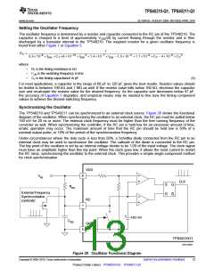
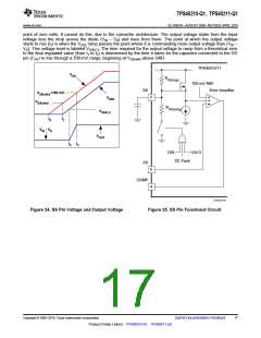
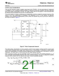
point of zero volts. It cannot do this, due to the converter architecture. The output voltage starts from the input
voltage less the drop across the diode (VIN – VD) and rises from there. The point at which the output voltage
starts to rise (t2) is when the VSSE ramp passes the point where it is commanding more output voltage than (VIN
–
VD). This voltage level is labeled VSSE(1). The time required for the output voltage to ramp from a theoretical zero
to the final regulated value (from t1 to t3) is determined by the time it takes for the capacitor connected to the SS
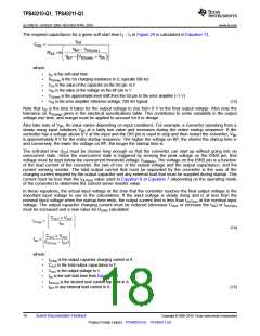
pin (CSS) to rise through a 700-mV range, beginning at VSS(ofst) above GND.
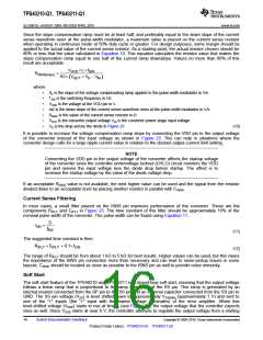
TPS40210/11
V
SS
R
SS(chg)
700 mV REF
SS
Error Amplifier
V
+700 mV
SS(ofst)
2
V
+
+
SSE
V
SS(ofst)
R
SS(dchg)
V
SSE(1)
t
t
1
0
V
- V
D
IN
V
OUT
t
t
3
2
DIS
UVLO
OC Fault
FB
5
4
COMP
UDG-07121
Figure 24. SS Pin Voltage and Output Voltage
Figure 25. SS Pin Functional Circuit
Copyright © 2008–2010, Texas Instruments Incorporated
Submit Documentation Feedback
17
Product Folder Link(s): TPS40210-Q1 TPS40211-Q1

 TI [ TEXAS INSTRUMENTS ]