TPS40210-Q1, TPS40211-Q1
www.ti.com
SLVS861D –AUGUST 2008–REVISED APRIL 2010
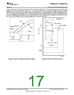
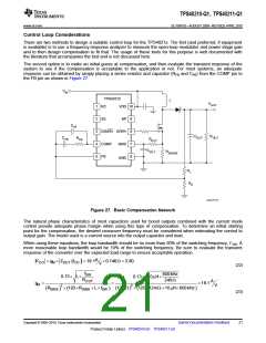
Control Loop Considerations
There are two methods to design a suitable control loop for the TPS4021x. The first (and preferred, if equipment
is available) is to use a frequency-response analyzer to measure the open-loop modulator and power stage gain
and to then design compensation to fit that. The usage of these tools for this purpose is well documented with
the literature that accompanies the tool and is not discussed here.
The second option is to make an initial guess at compensation, and then evaluate the transient response of the
system to see if the compensation is acceptable to the application or not. For most systems, an adequate
response can be obtained by simply placing a series resistor and capacitor (RFB and CFB) from the COMP pin to
the FB pin as shown in Figure 27.
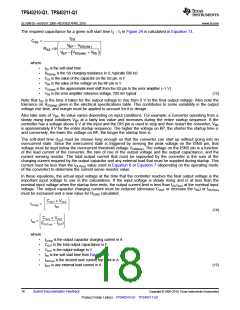
V
IN
TPS40210
L
V
OUT
1
2
3
4
5
RC
SS
VDD 10
BP
9
8
7
6
C
HF
DIS/EN GDRV
C
R
OUT
C
OUT
R
FB
R
FB
IFLT
COMP
FB
ISNS
GND
C
R
IFLT
SENSE
R
1
R
2
UDG-07177
Figure 27. Basic Compensation Network
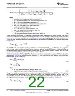
The natural phase characteristics of most capacitors used for boost outputs combined with the current mode
control provide adequate phase margin when using this type of compensation. To determine an initial starting
point for the compensation, the desired crossover frequency must be considered when estimating the control to
output gain. The model used is a current source into the output capacitor and load.
When using these equations, the loop bandwidth should be no more than 20% of the switching frequency, f SW. A
more reasonable loop bandwidth would be 10% of the switching frequency. Be sure to evaluate the transient
response of the converter over the expected load range to ensure acceptable operation.
A
KCO = gM ´ ZOUT
f
(CO )
= 19.1
´0.146W = 2.80
V
(22)
fSW
600kHz
0.13´ L ´
2 ´ 120´R
0.13´ 10mH´
ROUT
240W
A
gM
=
=
(
)
= 19.1
V
R
(
+ L ´ fSW
12mW 2 ´ 120´12mW +10mH´ 600kHz
) (
)
ISNS ) (
ISNS
(23)
Copyright © 2008–2010, Texas Instruments Incorporated
Submit Documentation Feedback
21
Product Folder Link(s): TPS40210-Q1 TPS40211-Q1

 TI [ TEXAS INSTRUMENTS ]