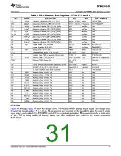
TPS40200-Q1
www.ti.com
SLUS739D –SEPTEMBER 2006–REVISED JULY 2011
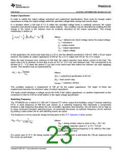
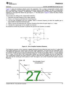
Figure 41 shows the feedback network used in this application. This is a type-2 compensation network, which
gives a combination of good transient response and phase boost for good stability. This type of compensation
has a pole at the origin, causing a –20-dB/decade (–1) slope, followed by a zero that causes a region of flat gain,
followed by a final pole that returns the gain slope to –1. The Bode plot in Figure 42 shows the effect of these
poles and zeros.
The procedure for setting up the compensation network is:
1. Determine the break frequency of the output capacitor.
2. Select a zero frequency well below this break frequency.
3. From the gain bandwidth of the error amplifier, select a crossover frequency at which the amplifier gain is
large relative to expected closed-loop gain.
4. Select a second zero well above the crossover frequency that returns the gain slope to a –1 slope.
5. Calculate the required gain for the amplifier at crossover.
Be prepared to iterate this procedure to optimize the pole and zero locations as needed.
C7
C8
R8
R10
+
R6
VREF
Figure 41. Error Amplifier Feedback Elements
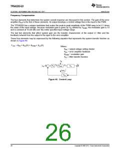
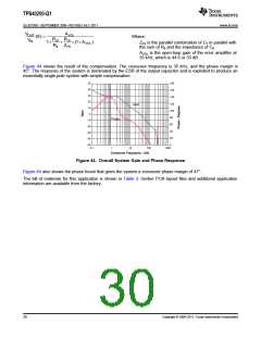
The frequency response of this converter is largely determined by two poles that arise from the LC output filter
and a higher-frequency zero caused by the ESR of the output capacitance. The poles from the output filter cause
a 40-dB/decade rolloff with a phase shift approaching 180°, followed by the output capacitor zero that reduces
the roll off to –20 dB and gives a phase boost back toward 90°. In other nomenclature, this is a –2 slope followed
by a –1 slope. The two zeros in the compensation network act to cancel the double pole from the output filter.
The compensation network’s two poles produce a region in which the error amplifier is flat and can be set to a
gain such that the overall gain of the system is 0 dB. This region is set so that it brackets the system crossover
frequency.
Gain - dB
Error Amplifier Type 2
Compensation
P
1
Slope = -1
z 1
p 2
AV2
Freq.
AV1
f1
f2
Figure 42. Error Amplifier Bode Plot
Copyright © 2006–2011, Texas Instruments Incorporated
27

 TI [ TEXAS INSTRUMENTS ]