TPS40200-Q1
www.ti.com
SLUS739D –SEPTEMBER 2006–REVISED JULY 2011
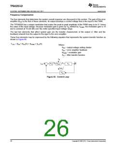
Output Capacitance
In order to satisfy the output voltage overshoot and undershoot specifications, there must be enough output
capacitance to keep the output voltage within the specified voltage limits during load current steps.
In a situation where a full load of 2.5 A within the specified voltage limits is suddenly removed, the output
capacitor must absorb energy stored in the output inductor. This condition may be described by realizing that the
energy in the stored in the inductor must be suddenly absorbed by the output capacitance. This energy
relationship is written as:
1
2
1
2
2
2
2
[ (
VOS - VO )]
´ LOIO
£
´
CO
Where:
VOS = allowed over-shoot voltage above the output voltage
LO = inductance
IO = output current
CO = output capacitance
VO = output voltage
In this application, the worst-case load step is 2.25 A, and the allowed overshoot is 100 mV. With a 33-μH output
inductor, this implies an output capacitance of 249 μF for a 3.3-V output and 165 μF for a 5-V output.
When the load increases from minimum to full load, the output capacitor must deliver current to the load. The
worst case is for a minimum on time that occurs at 16 V in, 3.3 V out, and minimum load. This corresponds to an
off time of (1 – 0.2) times the period 3.3 μs and is the worst-case time before the inductor can start supplying
current. This situation may be represented by:
tOFFMAX
DVO < DIO ´
Where:
CO
ΔVO = undershoot specification of 60 mV
ΔIO = load current step
tOFFMAX = maximum off time
This condition produces a requirement of 100 μF for the output capacitance. The larger of these two
requirements becomes the minimum value of output capacitance.
The ripple current develops a voltage across the ESR of the output capacitance, so another requirement on this
component is that its ESR be small relative to the ripple voltage specification.
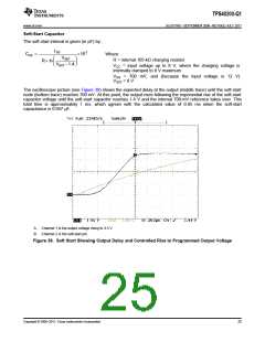
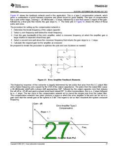
Switching Frequency
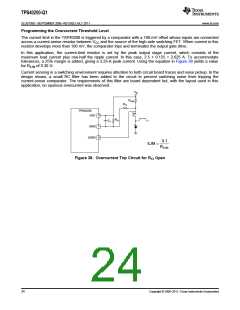
The TPS40200 has a built-in 8-V 200-mA P-channel FET-driver output that facilitates using P-channel switching
FETs. A clock frequency of 300 kHz was chosen as a switching frequency that represents a compromise
between a high frequency that allows the use of smaller capacitors and inductors, but one that is not so high as
to cause excessive transistor switching losses. As previously discussed, an optimum frequency can be selected
by picking a value where the dc and switching losses are equal.
The frequency is set by using the design formula given in the FET Selection Criteria section.
1
R
RC ´CRC =
Where:
RRC = timing resistor value in ohms or RRC = 68.1 kΩ
0.105´ fSW
CRC = timing capacitor value in F or C5 = 470 pF
fSW = desired switching frequency in Hz, which in this case
calculates to 297 kHz
At a worst case of 16 V, the timing resistor draws about 250 μA, which is well below the 750-μA maximum that
the circuit can pull down.
Copyright © 2006–2011, Texas Instruments Incorporated
23

 TI [ TEXAS INSTRUMENTS ]