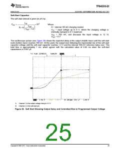
TPS40200-Q1
www.ti.com
SLUS739D –SEPTEMBER 2006–REVISED JULY 2011
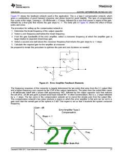
Step 5
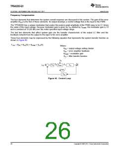
Calculate the gain elements in the system to determine the gain required by the error amplifier to make the
overall gain 0 dB at 35 kHz:
TV(S) = KFB ´ KEA (S)´KPWM ´ XLC (S)
Where:
KFB is the output voltage setting divider
KEA is the error amplifier feedback
KPWM is the modulator gain
XLC is the filter transfer function
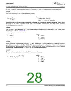
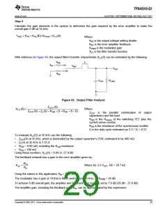
With reference to Figure 43, the output filter's transfer characteristic XLC(S) can be estimated by the following:
L
RSW
VIN
D
VSW
VOUT
1-D
RSR
RLOAD
COUT
Figure 43. Output Filter Analysis
ZOUT (S)
ZOUT (S) + ZL(S) + RSW ´ D + RSR ´ (1- D)
XLC (S) =
Where:
ZOUT is the parallel combination of output
capacitor(s) and the load
RSW is the RDS(on) of the switching FET plus the
current-sense resistor
RSR is the resistance of the synchronous rectifier
D is the duty cycle estimated as 3.3 / 12 = 0.27
To evaluate XLC(S) at 35 kHz use the following:
•
•
•
•
ZOUT(S) at 35 kHz, which is dominated by the output capacitorr's ESR; estimated to be 400 mΩ
ZL(S) at 35 KHz is 7.25 Ω
RSW = 0.95 mΩ, including the RLIM resistance
RSR = 100 mΩ
Using these numbers, XLC(S) = 0.04 or -27.9 dB.
The feedback network has a gain to the error amplifier given by:
R10
Kfb
=
Where for 3.3 VOUT, R6 = 26.7 kΩ
R6
Using the values in this application, Kfb = 11.4 dB.
The modulator has a gain of 10 that is flat to well beyond 35 kHz, so KPWM = 20 dB.
To acheive 0 dB overall gain, the amplifier and feedback gain must be set to 7.9 dB (20 dB - 27.9 dB)
The amplifier gain, including the feedback gain, Kfb, can be approximated by this expression:
Copyright © 2006–2011, Texas Instruments Incorporated
29

 TI [ TEXAS INSTRUMENTS ]