TPS40200-Q1
SLUS739D –SEPTEMBER 2006–REVISED JULY 2011
www.ti.com
Frequency Compensation
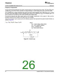
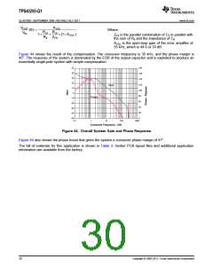
The four elements that determine the system overall response are discussed in this section. The gain of the error
amplifier (KEA) is the first of these elements. Its output develops a control voltage that is the input to the PWM.
The TPS40200 has a unique modulator that scales the peak-to-peak amplitude of the PWM ramp to be 0.1 times
the value of the input voltage. Because modulator gain is given by VIN divided by VRAMP, the modulator gain is 10
and is constant at 10 (20 dB) over the entire specified input-voltage range.
The last two elements that affect system gain are the transfer characteristic of the output LC filter and the
feedback network from the output to the input to the error amplifier.
These four elements may be expressed by the following equation that represents the system transfer function as
shown in Figure 40.
TV(S) = KFB × KEA(S) × KPWM × XLC(S)
Where:
KFB = output voltage setting divider
KEA = error amplifier feedback
KPWM = modulator gain
XLC = filter transfer function
v
g
v
v
o
c
+
d
KEA
KPWM
XLC
Vref
-
Tv(s)
KFB
Figure 40. Control Loop
26
Copyright © 2006–2011, Texas Instruments Incorporated

 TI [ TEXAS INSTRUMENTS ]