TPS40200-Q1
www.ti.com
SLUS739D –SEPTEMBER 2006–REVISED JULY 2011
Component Selection
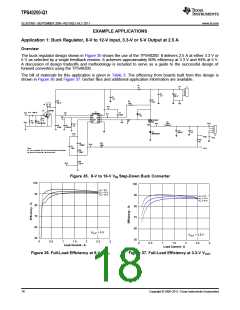
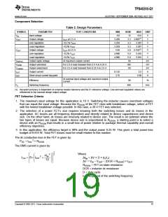
Table 2. Design Parameters
SYMBOL
VIN
VOUT
PARAMETER
TEST CONDITIONS
MIN
8.0
NOM
MAX
UNIT
V
Input voltage
12
16.0
Output voltage
IOUT at 2.5 A
3.200
3.293
3.293
4.85
3.3 3.400(1)
V
Line regulation
~0.2 % VOUT
3.3
3.3
3.307
3.307
V
Load regulation
Output voltage
~0.2% VOUT
V
VOUT
IOUT at 2.5 A
5.0 5.150(1)
V
Line regulation
~0.2% VOUT
4.990
4.990
5.0
5.0
60
5.010
5.010
V
Load regulation
Output ripple voltage
Output overshoot
Output undershoot
Output current
~0.2% VOUT
V
VRIPPLE
VOVER
VUNDER
IOUT
At maximum output current
For 2.5-A load transient from 2.5 A to 0.25 A
For 2.5-A load transient from 0.25 A to 2.5 A
mV
mV
mV
A
100
60
0.125
3.75
2.5
ISCP
Short-circuit current trip point
5.00
A
At nominal input voltage and maximum output
current
Efficiency
90
%
FS
Switching frequency
300
kHz
(1) Set-point accuracy is dependent on external resistor tolerance and the IC reference voltage. Line and load regulation values are
referenced to the nominal design output voltage.
FET Selection Criteria
1. The maximum input voltage for this application is 16 V. Switching the inductor causes overshoot voltages
that can equal the input voltage. Because the RDSON of the FET rises with breakdown voltage, select a FET
with the lowest breakdown voltage possible. In this case, a 30-V FET was selected.
2. The selection of a power FET’s size requires knowing both the switching losses and dc losses in the
application. AC losses are all frequency dependent and directly related to device capacitances and device
size. On the other hand, dc losses are inversely related to device size. The result is an optimum where the
two types of losses are equal. Because device size is proportional to RDSON, a starting point is to select a
device with an RDSON that results in a small loss of power relative to package thermal capability and overall
efficiency objectives.
3. In this application, the efficiency target is 90% and the output power 8.25 W. This gives a total power-loss
budget of 0.916 W. Total FET losses must be small relative to this number.
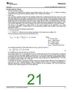
The dc conduction loss in the FET is given by:
PDC = Irms 2 × RDSON
The RMS current is given by:
1
2
Where:
ΔIpp = ΔV × D × (ts/LI)
2
é
ù
ú
æ
ç
ö
÷
DIpp
2
rms = D´ IOUT +
ê
I
ç
è
ë
÷
ø
ê
12
ú
û
ΔV = VIN – VOUT – (DCR + RDSON) × IOUT
RDSON = FET on-state resistance
DCR = inductor dc resistance
D = duty cycle
tS = reciprocal of the switching frequency
Copyright © 2006–2011, Texas Instruments Incorporated
19

 TI [ TEXAS INSTRUMENTS ]