TPS40200-Q1
www.ti.com
SLUS739D –SEPTEMBER 2006–REVISED JULY 2011
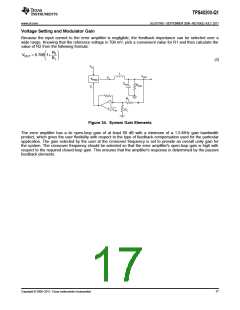
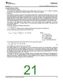
Rectifier Selection Criteria
•
Rectifier breakdown voltage
The rectifier must withstand the maximum input voltage, which, in this case, is 16 V. To allow for switching
transients that can approach the switching voltage, a 30-V rectifier was selected.
•
Diode size
The importance of power losses from the Schottky rectifier (D2) is determined by the duty cycle. For a low
duty-cycle application, the rectifier is conducting most of the time, and the current that flows through it times
its forward drop can be the largest component of loss in the entire controller. In this application, the duty cycle
ranges from 20% to 40%, which, in the worst case, means that the diode is conducting 80% of the time.
Where efficiency is of paramount importance, choose a diode with as low a forward drop as possible. In more
cost-sensitive applications, size may be reduced to the point of the thermal limitations of the diode package.
The device in this application is large relative to the current required by the application. In a more
cost-sensitive application, a smaller diode in a less-expensive package could provide a less-efficient but
appropriate solution.
The device used has the following characteristics:
•
•
Vf = 0.3 V at 3 A
Ct = 300 pF (Ct = effective reverse voltage capacitance of the synchronous rectifier, D2)
The two components of the losses from the diode D2 are:
IRIPPLE
Where:
D = the duty cycle
PCOND = Vf × IOUT
+
× (1 – D) = 653 mW
(
4
IRIPPLE = ripple current
IOUT = output current
VF = forward voltage
PCOND = conduction power loss
The switching capacitance of this diode adds an ac loss, given by Equation 7:
1
2
PSW
=
C× (V + V ) × f = 6.8 mW
IN
f
2
(7)
This additional loss raises the total loss to 660 mW.
At an output voltage of 3.3 V, the application runs at a nominal duty cycle of 27%, and the diode is conducting
72.5% of the time. As the output voltage is moved up to 5 V, the on time increases to 46%, and the diode is
conducting only 54% of the time during each clock cycle. This change in duty cycle proportionately reduces
the conduction power losses in the diode. This reduction may be expressed as 660(0.54/0.725) = 491 mW,
for a savings in power of 660 – 491 = 169 mW.
To illustrate the relevance of this power savings, measure the full-load module efficiency for this application at
3.3 V and 5 V. The 5-V output efficiency is 92%, compared to 89% for the 3.3-V design. This difference in
efficiency represents a 456-mW reduction in losses between the two conditions. This 169-mW power-loss
reduction in the rectifier represents 37% of the difference.
Copyright © 2006–2011, Texas Instruments Incorporated
21

 TI [ TEXAS INSTRUMENTS ]