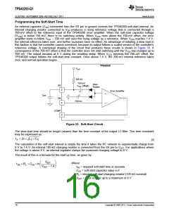
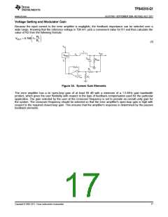
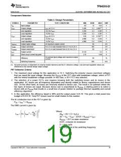
TPS40200-Q1
SLUS739D –SEPTEMBER 2006–REVISED JULY 2011
www.ti.com
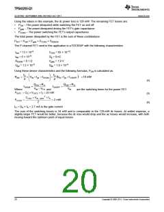
Using the values in this example, the dc power loss is 129 mW. The remaining FET losses are:
•
•
•
PSW – The power dissipated while switching the FET on and off
Pgate – The power dissipated driving the FET's gate capacitance
PCOSS – The power switching the FET's output capacitance
The total power dissipated by the FET is the sum of these contributions:
PFET = PSW + Pgate + PCOSS + PRDSON
The P-channel FET used in this application is a FDC654P with the following characteristics:
trise = 13 × 10–9
tfall = 6 × 10⁻⁹
COSS = 83 × 10–12
Qg = 9 nC
RDSON = 0.1 Ω
Qgd = 1.2 × 10⁻⁹
Vgate = 1.9 V
Qgs = 1.0 × 10⁻⁹
Using these device characteristics and the following formulas, PSW is calculated as:
æ
ö
fS
2
fS
ç
÷
PSW
=
´ VIN
´
´ tCHON + (VIN ´Ipk ´ tCHOFF ) =10 mW
Ipk
ç
è
÷
ø
2
(4)
QGD ´RG
VIN - VTH
QGD ´RG
tCHON
=
tCHOFF =
VIN
Where
and
are the switching times for the power FET.
PGATE = QG × VGATE × fS = 22 mW
(5)
(6)
2
COSS × VIN _MAX × fS
PCOSS
=
= 2 mW
2
IG = QG × fS = 2.7 mA is the gate current.
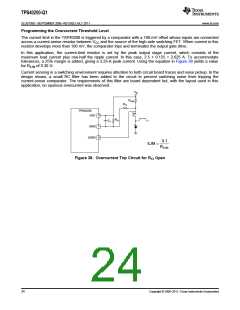
The sum of the switching losses is 34 mW and is comparable to the 129-mW dc losses. At added expense, a
slightly larger FET would be better, because the dc loss would drop and the ac losses would increase, with both
moving toward the optimum point of equal losses.
20
Copyright © 2006–2011, Texas Instruments Incorporated

 TI [ TEXAS INSTRUMENTS ]