TPS23753A
www.ti.com
SLVS933B –JULY 2009–REVISED JANUARY 2010
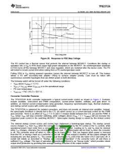
Figure 20. Response to PSE Step Voltage
The PD control has a thermal sensor that protects the internal hotswap MOSFET. Conditions like startup or
operation into a VDD to RTN short cause high power dissipation in the MOSFET. An overtemperature shutdown
(OTSD) turns off the hotswap MOSFET and class regulator, which are restarted after the device cools. The PD
will restart in inrush current limit when exiting from a PD overtemperature event.
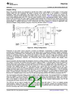
Pulling DEN to VSS during powered operation causes the internal hotswap MOSFET to turn off. This feature
allows a PD with secondary-side adapter ORing to achieve adapter priority. Care must be taken with
synchronous converter topologies that can deliver power in both directions.
The hotswap switch will be forced off under the following conditions:
•
•
•
•
VAPD above VAPDEN (~1.5 V)
DE N ≤ VPD_DIS when VVDD-VSS is in the operational range
PD over temperature
V
VVDD-VSS < PoE UVLO (~30.5 V).
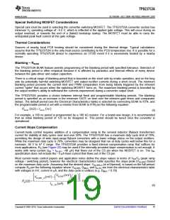
Converter Controller Features
The TPS23753A dc/dc controller implements a typical current-mode control as shown in Figure 2. Features
include oscillator, overcurrent and PWM comparators, current-sense blanker, softstart, and gate driver. In
addition, an internal current-compensation ramp generator, frequency synchronization logic, thermal shutdown,
and startup current source with control are provided.
The TPS23753A is optimized for isolated converters, and does not provide an internal error amplifier. Instead,
the optocoupler feedback is directly fed to the CTL pin which serves as a current-demand control for the PWM
and converter. There is an offset of VZDC (~1.5 V) and 2:1 resistor divider between the CTL pin and the PWM. A
VCTL below VZDC will stop converter switching, while voltages above (VZDC + 2 × VCSMAX) will not increase the
requested peak current in the switching MOSFET. Optocoupler biasing design is eased by this limited control
range.
The internal startup current source and control logic implement a bootstrap-type startup. The startup current
source charges CVC from VDD1 when the converter is disabled (either by the PD control or the VC control), while
operational power must come from a converter (bias winding) output. Loading on VC and VB must be minimal
while CVC charges, otherwise the converter may never start. The optocoupler will not load VB when the converter
is off. The converter shuts off when VC falls below its lower UVLO. This can happen when power is removed
from the PD, or during a fault on a converter output rail. When one output is shorted, all the output voltages fall
including the one that powers VC. The control circuit discharges VC until it hits the lower UVLO and turns off. A
restart will initiate as described in "Startup and Converter Operation" if the converter turns off and there is
sufficient VDD1 voltage. This type of operation is sometimes referred to as “hiccup mode,” which provides robust
output short protection by providing time-average heating reduction of the output rectifier.
Copyright © 2009–2010, Texas Instruments Incorporated
Submit Documentation Feedback
17

 TI [ TEXAS INSTRUMENTS ]