TPS23753A
www.ti.com
SLVS933B –JULY 2009–REVISED JANUARY 2010
Special Switching MOSFET Considerations
Special care must be used in selecting the converter switching MOSFET. The TPS23753A converter section has
minimum VC operating voltage of ~5.5 V, which is reflected in the applied gate voltage. This will occur during an
output overload, or towards the end of a (failed) bootstrap startup. The MOSFET must be able to carry the
anticipated peak fault current at this gate voltage.
Thermal Considerations
Sources of nearby local PCB heating should be considered during the thermal design. Typical calculations
assume that the TPS23753A is the only heat source contributing to the PCB temperature rise. It is possible for a
normally operating TPS23753A device to experience an OTSD event if it is excessively heated by a nearby
device.
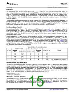
Blanking – RBLNK
The TPS23753A BLNK feature permits programming of the blanking period with specified tolerance. Selection of
the blanking period is often empirical because it is affected by parasitics and thermal effects of every device
between the gate-driver and output capacitors.
There is a critical range of blanking period that is bounded on the short side by erratic operation, and on the long
side by potentially harmful switching-MOSFET and output rectifier currents during a short circuit. The minimum
blanking period prevents the current limit and PWM comparators from being falsely triggered by the inherent
current “spike” that occurs when the switching MOSFET turns on. The maximum blanking period is bounded by
the output rectifier's ability to withstand the currents experienced during a converter output short.
The TPS23753A provides a choice between internal fixed and programmable blanking periods. The blanking
period is specified as an increase in the minimum GATE on time over the inherent gate driver and comparator
delays. The default period (see the Electrical Characteristics table) is selected by connecting BLNK to RTN, and
the programmable period is set with a resistor from BLNK to RTN per the following equation.
R
kΩ = t
( )
ns
BLNK
( )
BLNK
(5)
For example, a 100 ns period is programmed by a 100 kΩ resistor. For a brand-new design, it is recommended
that an initial blanking period of 125 ns be designed in. This period should be tuned once the converter is
operational.
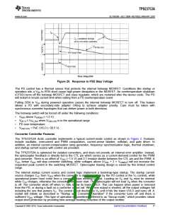
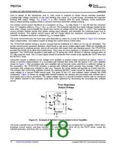
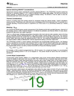
Current Slope Compensation
Current-mode control requires addition of a compensation ramp to the sensed inductor (flyback transformer)
current for stability at duty cycles near and over 50%. The TPS23753A has a maximum duty cycle limit of 78%,
permitting the design of wide input-range flyback converters with a lower voltage stress on the output rectifiers.
While the maximum duty cycle is 78%, converters may be designed that run at duty cycles well below this for a
narrower, 36 V to 57 V range. The TPS23753A provides a fixed internal compensation ramp that suffices for
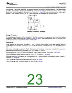
most applications. RS (see Figure 22) may be used if the internally provided slope compensation is not enough. It
works with ramp current (IPK = ISL-EX, ~40 mA) that flows out of the CS pin when the MOSFET is on. The IPK
specification does not include the ~3 mA fixed current that flows out of the CS pin.
Most current-mode control papers and application notes define the slope values in terms of VPP/TS (peak ramp
voltage / switching period), however the electrical characteristics table specifies the slope peak (VSLOPE) based
on the maximum duty cycle. Assuming that the desired slope, VSLOPE-D (in mV/period), is based on the full period,
compute RS per the following equation where VSLOPE, DMAX, and ISL-EX are from the electrical characteristics table
with voltages in mV, current in mA, and the duty cycle is unitless (e.g. DMAX = 0.78).
V
(mV)
SLOPE
VSLOPE _D(mV) −
D
MAX
RS(Ω) =
⋅1000
ISL _EX (µA)
(6)
19
Copyright © 2009–2010, Texas Instruments Incorporated
Submit Documentation Feedback

 TI [ TEXAS INSTRUMENTS ]