TPS23753A
www.ti.com
SLVS933B –JULY 2009–REVISED JANUARY 2010
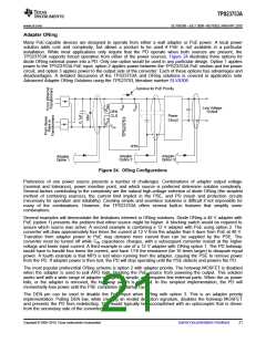
Adapter ORing
Many PoE-capable devices are designed to operate from either a wall adapter or PoE power. A local power
solution adds cost and complexity, but allows a product to be used if PoE is not available in a particular
installation. While most applications only require that the PD operate when both sources are present, the
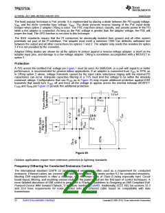
TPS23753A supports forced operation from either of the power sources. Figure 24 illustrates three options for
diode ORing external power into a PD. Only one option would be used in any particular design. Option 1 applies
power to the TPS23753A PoE input, option 2 applies power between the TPS23753A PoE section and the power
circuit, and option 3 applies power to the output side of the converter. Each of these options has advantages and
disadvantages. A detailed discussion of the TPS23753A and ORing solutions is covered in application note
Advanced Adapter ORing Solutions using the TPS23753, literature number SLVA306.
Optional for PoE Priority
Low Voltage
Output
DEN
CLS
Power
Circuit
VSS
5/8/08
RTN
Adapter
Option 2
Adapter
Option 3
Adapter
Option 1
Figure 24. ORing Configurations
Preference of one power source presents a number of challenges. Combinations of adapter output voltage
(nominal and tolerance), power insertion point, and which source is preferred determine solution complexity.
Several factors contributing to the complexity are the natural high-voltage selection of diode ORing (the simplest
method of combining sources), the current limit implicit in the PSE, and PD inrush and protection circuits
(necessary for operation and reliability). Creating simple and seamless solutions is difficult if not impossible for
many of the combinations. However, the TPS23753A offers several built-in features that simplify some
combinations.
Several examples will demonstrate the limitations inherent in ORing solutions. Diode ORing a 48 V adapter with
PoE (option 1) presents the problem that either source might be higher. A blocking switch would be required to
assure which source was active. A second example is combining a 12 V adapter with PoE using option 2. The
converter will draw approximately four times the current at 12 V from the adapter than it does from PoE at 48 V.
Transition from adapter power to PoE may demand more current than can be supplied by the PSE. The
converter must be turned off while CIN capacitance charges, with a subsequent converter restart at the higher
voltage and lower input current. A third example is use of a 12 V adapter with ORing option 1. The PD hotswap
would have to handle four times the current, and have 1/16 the resistance (be 16 times larger) to dissipate equal
power. A fourth example is that MPS is lost when running from the adapter, causing the PSE to remove power
from the PD. If adapter power is then lost, the PD will stop operating until the PSE detects and powers the PD.
The most popular preferential ORing scheme is option 2 with adapter priority. The hotswap MOSFET is disabled
when the adapter is used to pull APD high, blocking the PoE source from powering the output. This solution
works well with a wide range of adapter voltages, is simple, and requires few external parts. When the ac power
fails, or the adapter is removed, the hotswap switch is enabled. In the simplest implementation, the PD will
momentarily lose power until the PSE completes its startup cycle.
The DEN pin can be used to disable the PoE input when ORing with option 3. This is an adapter priority
implementation. Pulling DEN low, while creating an invalid detection signature, disables the hotswap MOSFET
and prevents the PD from redetecting. This would typically be accomplished with an optocoupler that is driven
from the secondary side of the converter.
Copyright © 2009–2010, Texas Instruments Incorporated
Submit Documentation Feedback
21

 TI [ TEXAS INSTRUMENTS ]