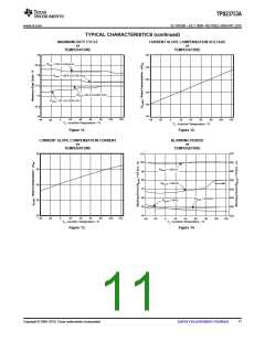
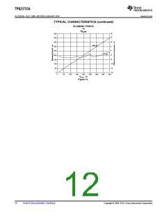
TPS23753A
www.ti.com
SLVS933B –JULY 2009–REVISED JANUARY 2010
Detection
The TPS23753A is in detection mode whenever VVDD-V SS is below the lower classification threshold. When the
input voltage rises above VCL_ON, the DEN pin goes to an open-drain condition to conserve power. While in
detection, RTN is high impedance, almost all the internal circuits are disabled, and the DEN pin is pulled to VSS
.
An RDEN of 24.9 kΩ (1%), presents the correct signature. It may be a small, low-power resistor since it only sees
a stress of about 5 mW. A valid PD detection signature is an incremental resistance between 23.75 kΩ and
26.25 kΩ at the PI.
The detection resistance seen by the PSE at the PI is the result of the input bridge resistance in series with the
parallel combination of RDEN and the TPS23753A bias loading. The input diode bridge’s incremental resistance
may be hundreds of Ohms at the very low currents drawn when 2.7 V is applied to the PI. The input bridge
resistance is partially cancelled by the TPS23753A's effective resistance during detection.
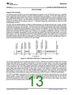
Hardware Classification
Hardware classification allows a PSE to determine a PD’s power requirements before starting and helps with
power management once power is applied. The maximum power entries in Table 2 determine the class the PD
must advertise. A Type 1 PD may not advertise Class 4. The PSE may disconnect a PD if it draws more than its
stated Class power. The standard permits the PD to draw limited current peaks, however the average power
requirement always applies.
Voltage between 14.5 V and 20.5 V is applied to the PD for up to 75 ms during hardware Classification. A fixed
output voltage is sourced by the CLS pin, causing a fixed current to be drawn from VDD through RCLS. The total
current drawn from the PSE during classification is the sum of bias and RCLS currents. PD current is measured
and decoded by the PSE to determine which of the five available classes is advertised (see Table 2). The
TPS23753A disables classification above VCU_OFF to avoid excessive power dissipation. CLS voltage is turned off
during PD thermal limit or when APD or DEN are active. The CLS output is inherently current limited, but should
not be shorted to VSS for long periods of time.
Table 2. Class Resistor Selection
POWER AT PD PI
Class Current Requirement
CLASS
RESISTOR (Ω)
NOTES
MINIMUM
MAXIMUM
MINIMUM (mA)
MAXIMUM (W)
(W)
0.44
0.44
3.84
6.49
12.95
(mA)
0
1
2
3
4
12.95
3.84
0
4
1270
243
9
12
20
30
44
6.49
17
26
36
137
12.95
25.5
90.9
63.4
Only permitted for type 2 devices
Maintain Power Signature (MPS)
The MPS is an electrical signature presented by the PD to assure the PSE that it is still present after operating
voltage is applied. A valid MPS consists of a minimum dc current of 10 mA (at a duty cycle of at least 75 ms on
every 225 ms) and an ac impedance lower than 26.25 kΩ in parallel with 0.05 mF. The ac impedance is usually
accomplished by the minimum CIN requirement of 5 mF. When APD or DEN are used to force the hotswap switch
off, the dc MPS will not be met. A PSE that monitors the dc MPS will remove power from the PD when this
occurs. A PSE that monitors only the ac MPS may remove power from the PD.
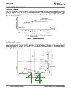
TPS23753A Operation
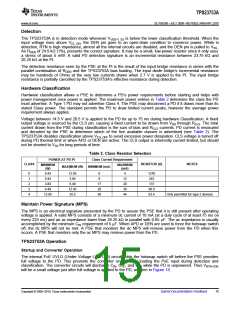
Startup and Converter Operation
The internal PoE UVLO (Under Voltage Lock Out) circuit holds the hotswap switch off before the PSE provides
full voltage to the PD. This prevents the converter circuits from loading the PoE input during detection and
classification. The converter circuits will discharge CIN, CVC, and CVB while the PD is unpowered. Thus VRTN-VDD
will be a small voltage just after full voltage is applied to the PD, as seen in Figure 18.
Copyright © 2009–2010, Texas Instruments Incorporated
Submit Documentation Feedback
15

 TI [ TEXAS INSTRUMENTS ]