TPS23753A
SLVS933B –JULY 2009–REVISED JANUARY 2010
www.ti.com
Care in design of the transformer and VC bias circuit is required to obtain hiccup overload protection.
Leading-edge voltage overshoot on the bias winding may cause VC to peak-charge, preventing the expected
tracking with output voltage. RVC (Figure 1) is often required slow the peak charging. Good transformer
bias-to-output-winding coupling results in reduced overshoot and better voltage tracking.
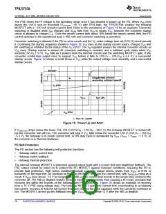
The startup current source transitions to a resistance as (VDD1 - VC) falls below 7 V, but will start the converter
from 12 V adapters within tST (VDD1 ≥ 10.2, tST~85 ms). The converter will start from lower voltages, limited by the
case when charge current equals the device bias current at voltage below the upper VC UVLO. The bootstrap
source provides reliable startup from widely varying input voltages, and eliminates the continual power loss of
external resistors. The startup current source will not charge above the maximum recommended VVC if the
converter is disabled and there is sufficient VDD1 to charge higher.
The peak current limit does not have duty cycle dependency unless RS is used as shown in Figure 22 to increase
slope compensation. This makes it easier to design the current limit to a fixed value.
The TPS23753A blanker timing is precise enough that the traditional R-C filters on CS can be eliminated. This
avoids current-sense waveform distortion, which tends to get worse at light output loads. While the internally set
blanking period is relatively precise, almost all converters will require their own blanking period. The TPS23753A
provides the BLNK pin to allow this programming. There may be some situations or designers that prefer an R-C
approach. The TPS23753A provides a pull-down on CS during the GATE off time to improve sensing when an
R-C filter must be used. The CS input signal should be protected from nearby noisy signals like GATE drive and
the MOSFET drain.
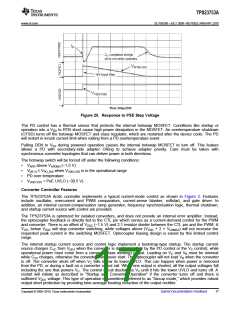
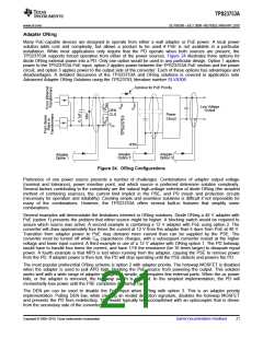
Converters require a softstart on the voltage error amplifier to prevent output overshoot on startup. Figure 21
shows a common implementation of a secondary-side softstart that works with the typical TL431 error amplifier
shown in Figure 1. This secondary-side error amplifier will not become active until there is sufficient voltage on
the secondary. The TPS23753A provides a primary-side softstart which persists long enough (~800 ms) for
secondary side voltage-loop softstart to take over, however the actual startup will typically be shorter than this.
The primary-side current-loop softstart controls the switching MOSFET peak current by applying a slowly rising
ramp voltage to a second PWM control input. The lower of the CTL and softstart ramps controls the PWM
comparator. Figure 19 shows an exaggerated handoff between the primary and secondary-side softstart that is
most easily seen in the IPI waveform. The output voltage rises in a smooth monotonic fashion with no overshoot.
The softstart handoff in this example could have been optimized by decreasing the secondary-side softstart
period.
From Regulated
Output Voltage
ROB
CIZ
RSS
RFBU
DSS
CSS
RFBL
TLV431
Figure 21. Example of Softstart Circuit Added to Error Amplifier
The dc/dc controller has an OTSD that can be triggered by heat sources including the VB regulator, GATE driver,
bootstrap current source, and bias currents. The controller OTSD turns off VB, the GATE driver, resets the
softstart generator, and forces the VC control into an under-voltage state.
18
Submit Documentation Feedback
Copyright © 2009–2010, Texas Instruments Incorporated

 TI [ TEXAS INSTRUMENTS ]