TMS3705
11-07-22-003 – SCBS881B –JANUARY 2010–REVISED APRIL 2010
www.ti.com
The default mode is a read-only mode that uses the default frequency as the carrier frequency for the full bridge.
Therefore the mode control register does not need to be written (it is filled with low states), and the
communication sequence between microcontroller and base station starts with TXCT being low for a fixed time to
initiate the charge phase. When TXCT becomes high again, the module enters the read phase and the data
transmission via the SCIO pin to the microcontroller starts.
There is another read-only mode that differs from the default mode only in the writing of the mode control register
before the start of the charge phase. The way that the mode control register is filled and the meaning of its
contents is described below.
The write-read mode starts with the programming of the mode control register. Then the charge phase starts with
TXCT being low for a fixed time. When TXCT becomes high again, the write phase begins in which the data are
transmitted from the microcontroller to the transponder via the TXCT pin, the control logic, the predrivers, and the
full bridge by amplitude modulation of 100% with a fixed delay time. After the write phase TXCT goes low again
to start another charge or program phase. When TXCT becomes high again, the read phase begins.
The contents of the mode control register define the mode and the way that the carrier frequency generated by
the frequency divider is selected in order to meet the transponder resonance frequency as good as possible.
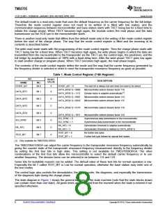
Table 1. Mode Control Register (7-Bit Register)
BIT
RESET
VALUE
DESCRIPTION
NAME
NO.
START_BIT
Bit 0
0
0
START_BIT = 0
DATA_BIT[4:1] = 0000
DATA_BIT[4:1] = 1111
DATA_BIT[4:1] = 0001
DATA_BIT[4:1] = 0010
...
The start bit is always low and does not need to be stored.
Microcontroller selects division factor 119
Division factor is adapted automatically(1)
Microcontroller selects division factor 114
Microcontroller selects division factor 115
...
DATA_BIT1
DATA_BIT2
DATA_BIT3
DATA_BIT4
SCI_SYNC
RX_AFC
Bit 1
Bit 2
Bit 3
Bit 4
Bit 5
Bit 6
Bit 7
0
0
0
0
0
0
DATA_BIT[4:1] = 0110
...
Microcontroller selects division factor 119
...
DATA_BIT[4:1] = 1011
SCI_SYNC = 0
SCI_SYNC = 1
RX_AFC = 0
Microcontroller selects division factor 124
Asynchronous data transmission to the microcontroller
Synchronous data transmission to the microcontroller
Demodulator threshold is adapted automatically
Demodulator threshold is defined by DATA_BIT[4:1]
No further test bytes
RX_AFC = 1
TEST_BIT = 0
TEST_BIT
TEST_BIT = 1
Further test byte follows for special test modes
(1) Only available for TMS3705A1DRG4
The TMS3705A1DRG4 can adjust the carrier frequency to the transponder resonance frequency automatically by
giving the counter state of the transponder resonance-frequency measurement directly to the frequency divider
by setting the first four bits in high state. This setting is not available for TMS3705BDRG4. The other
combinations of the first four bits allow the microcontroller to select the default carrier frequency or to use
another frequency. The division factor can be selected to be between 114 and 124.
Some bits for testability reasons can be added. The default value of these test bits for normal operation is low.
Especially the bit 7 called TEST_BIT is Low for normal operation; otherwise the base station may enter one of
the test modes.
The control logic also controls the demodulator, the SCI encoder, the diagnosis, and especially the transmission
of the diagnosis byte during the charge phase.
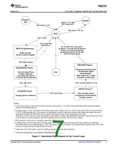
The state diagram in Figure 1 shows the general behavior of the state machine (note that the state blocks drawn
can contain more than one state). All given times are measured from the moment when the state is entered if not
specified otherwise.
8
Submit Documentation Feedback
Copyright © 2010, Texas Instruments Incorporated

 TI [ TEXAS INSTRUMENTS ]