TMS3705
11-07-22-003 – SCBS881B –JANUARY 2010–REVISED APRIL 2010
www.ti.com
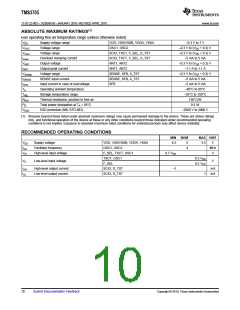
ABSOLUTE MAXIMUM RATINGS(1)
over operating free-air temperature range (unless otherwise noted)
VDD
Supply voltage range
VDD, VSS/VSSB, VDDA, VSSA
OSC1, OSC2
–0.3 V to 7 V
VOSC
Vinout
Iinout
VANT
IANT
Voltage range
–0.3 V to (VDD + 0.3) V
–0.3 V to (VDD + 0.3) V
–5 mA to 5 mA
Voltage range
SCIO, TXCT, F_SEL, D_TST
SCIO, TXCT, F_SEL, D_TST
ANT1, ANT2
Overload clamping current
Output voltage
–0.3 V to (VDD + 0.3) V
–1.1 A to 1.1 A
Output peak current
ANT1, ANT2
Vanalog
ISENSE
ISFB
Voltage range
SENSE, SFB, A_TST
SENSE, SFB, A_TST
SFB
–0.3 V to (VDD + 0.3) V
–5 mA to 5 mA
SENSE input current
Input current in case of overvoltage
Operating ambient temperature
Storage temperature range
Thermal resistance, junction to free air
Total power dissipation at TA = 85°C
ESD protection (MIL STD 883)
–5 mA to 5 mA
TA
–40°C to 85°C
Tstg
–55°C to 150°C
130°C/W
RqJA
PD
0.5 W
VESD
–2000 V to 2000 V
(1) Stresses beyond those listed under absolute maximum ratings may cause permanent damage to the device. These are stress ratings
only, and functional operation of the device at these or any other conditions beyond those indicated under recommended operating
conditions is not implied. Exposure to absolute-maximum-rated conditions for extended periods may affect device reliability.
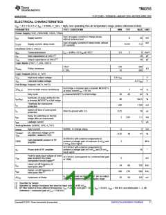
RECOMMENDED OPERATING CONDITIONS
MIN NOM
MAX UNIT
VDD
fosc
VIH
Supply voltage
VDD, VSS/VSSB, VDDA, VSSA
OSC1, OSC2
4.5
5
4
5.5
V
MHz
V
Oscillator frequency
High-level input voltage
F_SEL, TXCT, OSC1
TXCT, OSC1
0.7 VDD
0.3 VDD
0.2 VDD
VIL
Low-level input voltage
V
F_SEL
IOH
IOL
High-level output current
Low-level output current
SCIO, D_TST
–1
mA
mA
SCIO, D_TST
1
10
Submit Documentation Feedback
Copyright © 2010, Texas Instruments Incorporated

 TI [ TEXAS INSTRUMENTS ]