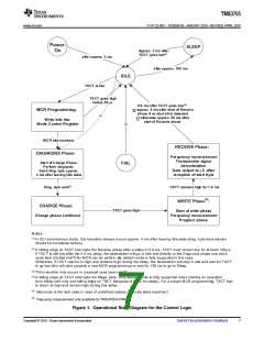
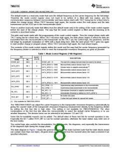
TMS3705
www.ti.com
11-07-22-003 – SCBS881B –JANUARY 2010–REVISED APRIL 2010
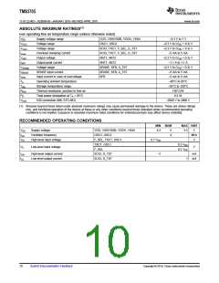
ELECTRICAL CHARACTERISTICS
VDD = 4.5 V to 5.5 V, fosc = 4 MHz, F_SEL = high, over operating free-air temperature range (unless otherwise noted)
PARAMETER
TEST CONDITIONS
MIN
TYP
MAX UNIT
Power Supply (VDD, VSS/VSSB, VDDA, VSSA)
Sum of supply currents in charge phase,
without antenna load
IDD
Supply current
8
20
mA
mA
Sum of supply currents in sleep mode, without
I/O currents
ISLEEP
Supply current, sleep mode
0.015
0.2
Oscillator (OSC1, OSC2)
gosc
Cin
Transconductance
fosc = 4 MHz, 0.5 Vpp at OSC1
0.5
2
5
10
10
mA/V
pF
Input capacitance at OSC1(1)
Output capacitance at OSC2(1)
Cout
pF
Logic Inputs (TXCT, F_SEL, OSC1)
Rpullup Pullup resistance
Logic Outputs (SCIO, D_TST)
TXCT
120
10
500
500
kΩ
F_SEL
VOH
VOL
High-level output voltage
Low-level output voltage
0.8 VDD
V
V
0.2 VDD
Full-Bridge Outputs (ANT1, ANT2)
Full bridge n-channel and p-channel MOSFETs
at driver current Iant = 50 mA
ΣRds_on
Sum of drain-source resistances
7
14
42
Ω
%
%
Duty cycle
p-channel MOSFETs of full bridge
38
96
40
Symmetry of pulse widths for the
p-channel MOSFETs of full bridge
ton1/ton2
Ioc
104.5
Threshold for overcurrent
protection
220
0.25
2
1100
10
mA
µs
Switch-off time of overcurrent
protection
toc
Short to ground with 3 Ω
Delay for switching on the full
bridge after an overcurrent
tdoc
2.05
2.1
1
ms
µA
Ileak
Leakage current
Analog Module (SENSE, SFB, A_TST)
ISENSE
Input current
SENSE, In charge phase
–2
2
mA
%
VDCREF
VDD
/
DC reference voltage of RF
amplifier, related to VDD
9.25
10
11
At 500 kHz with external components to
achieve a voltage gain of minimum 4-mVpp and
5-mVpp input signal
Gain-bandwidth product of RF
amplifier
GBW
fO
2
MHz
°
At 134 kHz with external components to
achieve a voltage gain of 5-mVpp and 20-mVpp
input signal
Phase shift of RF amplifier
16
Peak-to-peak input voltage of band
pass at which the limiter
At 134 kHz (corresponds to a minimal total gain
of 1000)
Vsfb
5
mV
comparator should toggle(2)
Lower cut-off frequency of
band-pass filter(3)
flow
24
160
25
60
270
50
100 kHz
500 kHz
Higher cut-off frequency of
band-pass filter(3)
fhigh
ΔVhys
A_TST pin used as input, D_TST pin as output,
Offset level determined by bandpass stage
Hysteresis of limiter
135
mV
(1) Specified by design
(2) Specified by design; functional test done for input voltage of 90 mVpp
.
(3) BP filter tested at three different frequencies: fmid =134 kHz and gain > 30 db; flow = 24 kHz, fhigh = 500 kHz and attenuation < –3 dB
(reference = measured gain at fmid = 134 kHz).
Copyright © 2010, Texas Instruments Incorporated
Submit Documentation Feedback
11

 TI [ TEXAS INSTRUMENTS ]