TMS3705
11-07-22-003 – SCBS881B –JANUARY 2010–REVISED APRIL 2010
www.ti.com
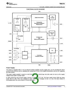
Oscillator
The oscillator generates the clock of the base station IC of which all timing signals are derived. Between its input
and output a crystal or ceramic resonator is connected that oscillates at a typical frequency of 4 MHz. If a digital
clock signal with a frequency of 4 MHz or 2 MHz is supplied to pin OSC1, the signal can be used to generate the
internal operation frequency of 16 MHz.
The oscillator block contains a PLL that generates the internal clock frequency of 16 MHz from the input clock
signal. The PLL multiplies the input clock frequency depending on the logic state of the input pin F_SEL by a
factor of 4 (F_SEL is high) or by a factor of 8 (F_SEL is low).
In sleep mode the oscillator is switched off.
Predrivers
The predrivers generate the signals for the four power transistors of the full bridge using the carrier frequency
generated by the frequency divider. The gate signals of the p-channel power transistors (active low) have the
same width (±1 cycle of the 16 MHz clock), the delay between one p-channel MOSFET being switched off and
the other one being switched on is defined to be 12 cycles of the 16 MHz clock. In write mode the first activation
of a gate signal after a bit pause is synchronized to the received transponder signal by a phase shift of 18°.
Full Bridge
The full bridge drives the antenna current at the carrier frequency during the charge phase and the active time of
the write phase. The minimal load resistance the full bridge sees between its outputs in normal operation at the
resonance frequency of the antenna is 43.3 Ω. When the full bridge is not active, the two driver outputs are
switched to ground.
Both outputs of the full bridge are protected independently against short-circuits to ground.
In case of an occurring short-circuit, the full bridge is switched off in less than 10 µs in order to avoid a drop of
the supply voltage. After a delay time of less than 10 ms the full bridge is switched on again to test if the
short-circuit is still there. An overcurrent due to a resistive short to ground that is higher than the maximum
current in normal operation but lower than the current threshold for overcurrent protection does not need to be
considered.
RF Amplifier
The RF amplifier is an operational amplifier with a fixed internal voltage reference and a voltage gain of 5 defined
by external resistors. It has a high gain-bandwidth product of at least 2 MHz in order to show a phase shift of less
than 16° for the desired signal and to give the possibility to use it as a low-pass filter by adapting additional
external components.
The input signal of the RF amplifier is DC coupled to the antenna. The amplitude of the output signal of the RF
amplifier is higher than 5 mV peak-to-peak.
Band-Pass Filter and Limiter
The band-pass filter provides amplification and filtering without external components. The lower cut-off frequency
is about a factor of 2 lower than the average signal frequency of 130 kHz, the higher cut-off frequency is about a
factor of 2 higher than 130 kHz.
The limiter converts the analog sine-wave signal to a digital signal. It provides a hysteresis depending on the
minimal amplitude of its input signal. The duty cycle of its digital output signal is between 40% and 60%. The
band-pass filter and the limiter together have a high gain of at least 1000.
4
Submit Documentation Feedback
Copyright © 2010, Texas Instruments Incorporated

 TI [ TEXAS INSTRUMENTS ]